- 您現(xiàn)在的位置:買賣IC網(wǎng) > PDF目錄11766 > XRT94L33IB (Exar Corporation)IC MAPPER DS3/E3/STS-1 504TBGA PDF資料下載
參數(shù)資料
| 型號: | XRT94L33IB |
| 廠商: | Exar Corporation |
| 文件頁數(shù): | 80/465頁 |
| 文件大?。?/td> | 0K |
| 描述: | IC MAPPER DS3/E3/STS-1 504TBGA |
| 標準包裝: | 24 |
| 應用: | 網(wǎng)絡切換 |
| 接口: | 總線 |
| 電源電壓: | 3.14 V ~ 3.47 V |
| 封裝/外殼: | 504-LBGA |
| 供應商設備封裝: | 504-TBGA(35x35) |
| 包裝: | 托盤 |
| 安裝類型: | 表面貼裝 |
第1頁第2頁第3頁第4頁第5頁第6頁第7頁第8頁第9頁第10頁第11頁第12頁第13頁第14頁第15頁第16頁第17頁第18頁第19頁第20頁第21頁第22頁第23頁第24頁第25頁第26頁第27頁第28頁第29頁第30頁第31頁第32頁第33頁第34頁第35頁第36頁第37頁第38頁第39頁第40頁第41頁第42頁第43頁第44頁第45頁第46頁第47頁第48頁第49頁第50頁第51頁第52頁第53頁第54頁第55頁第56頁第57頁第58頁第59頁第60頁第61頁第62頁第63頁第64頁第65頁第66頁第67頁第68頁第69頁第70頁第71頁第72頁第73頁第74頁第75頁第76頁第77頁第78頁第79頁當前第80頁第81頁第82頁第83頁第84頁第85頁第86頁第87頁第88頁第89頁第90頁第91頁第92頁第93頁第94頁第95頁第96頁第97頁第98頁第99頁第100頁第101頁第102頁第103頁第104頁第105頁第106頁第107頁第108頁第109頁第110頁第111頁第112頁第113頁第114頁第115頁第116頁第117頁第118頁第119頁第120頁第121頁第122頁第123頁第124頁第125頁第126頁第127頁第128頁第129頁第130頁第131頁第132頁第133頁第134頁第135頁第136頁第137頁第138頁第139頁第140頁第141頁第142頁第143頁第144頁第145頁第146頁第147頁第148頁第149頁第150頁第151頁第152頁第153頁第154頁第155頁第156頁第157頁第158頁第159頁第160頁第161頁第162頁第163頁第164頁第165頁第166頁第167頁第168頁第169頁第170頁第171頁第172頁第173頁第174頁第175頁第176頁第177頁第178頁第179頁第180頁第181頁第182頁第183頁第184頁第185頁第186頁第187頁第188頁第189頁第190頁第191頁第192頁第193頁第194頁第195頁第196頁第197頁第198頁第199頁第200頁第201頁第202頁第203頁第204頁第205頁第206頁第207頁第208頁第209頁第210頁第211頁第212頁第213頁第214頁第215頁第216頁第217頁第218頁第219頁第220頁第221頁第222頁第223頁第224頁第225頁第226頁第227頁第228頁第229頁第230頁第231頁第232頁第233頁第234頁第235頁第236頁第237頁第238頁第239頁第240頁第241頁第242頁第243頁第244頁第245頁第246頁第247頁第248頁第249頁第250頁第251頁第252頁第253頁第254頁第255頁第256頁第257頁第258頁第259頁第260頁第261頁第262頁第263頁第264頁第265頁第266頁第267頁第268頁第269頁第270頁第271頁第272頁第273頁第274頁第275頁第276頁第277頁第278頁第279頁第280頁第281頁第282頁第283頁第284頁第285頁第286頁第287頁第288頁第289頁第290頁第291頁第292頁第293頁第294頁第295頁第296頁第297頁第298頁第299頁第300頁第301頁第302頁第303頁第304頁第305頁第306頁第307頁第308頁第309頁第310頁第311頁第312頁第313頁第314頁第315頁第316頁第317頁第318頁第319頁第320頁第321頁第322頁第323頁第324頁第325頁第326頁第327頁第328頁第329頁第330頁第331頁第332頁第333頁第334頁第335頁第336頁第337頁第338頁第339頁第340頁第341頁第342頁第343頁第344頁第345頁第346頁第347頁第348頁第349頁第350頁第351頁第352頁第353頁第354頁第355頁第356頁第357頁第358頁第359頁第360頁第361頁第362頁第363頁第364頁第365頁第366頁第367頁第368頁第369頁第370頁第371頁第372頁第373頁第374頁第375頁第376頁第377頁第378頁第379頁第380頁第381頁第382頁第383頁第384頁第385頁第386頁第387頁第388頁第389頁第390頁第391頁第392頁第393頁第394頁第395頁第396頁第397頁第398頁第399頁第400頁第401頁第402頁第403頁第404頁第405頁第406頁第407頁第408頁第409頁第410頁第411頁第412頁第413頁第414頁第415頁第416頁第417頁第418頁第419頁第420頁第421頁第422頁第423頁第424頁第425頁第426頁第427頁第428頁第429頁第430頁第431頁第432頁第433頁第434頁第435頁第436頁第437頁第438頁第439頁第440頁第441頁第442頁第443頁第444頁第445頁第446頁第447頁第448頁第449頁第450頁第451頁第452頁第453頁第454頁第455頁第456頁第457頁第458頁第459頁第460頁第461頁第462頁第463頁第464頁第465頁
XRT94L33
xr
Rev.1.2.0.
3-CHANNEL DS3/E3/STS-1 TO STS-3/STM-1 MAPPER IC DATA SHEET
170
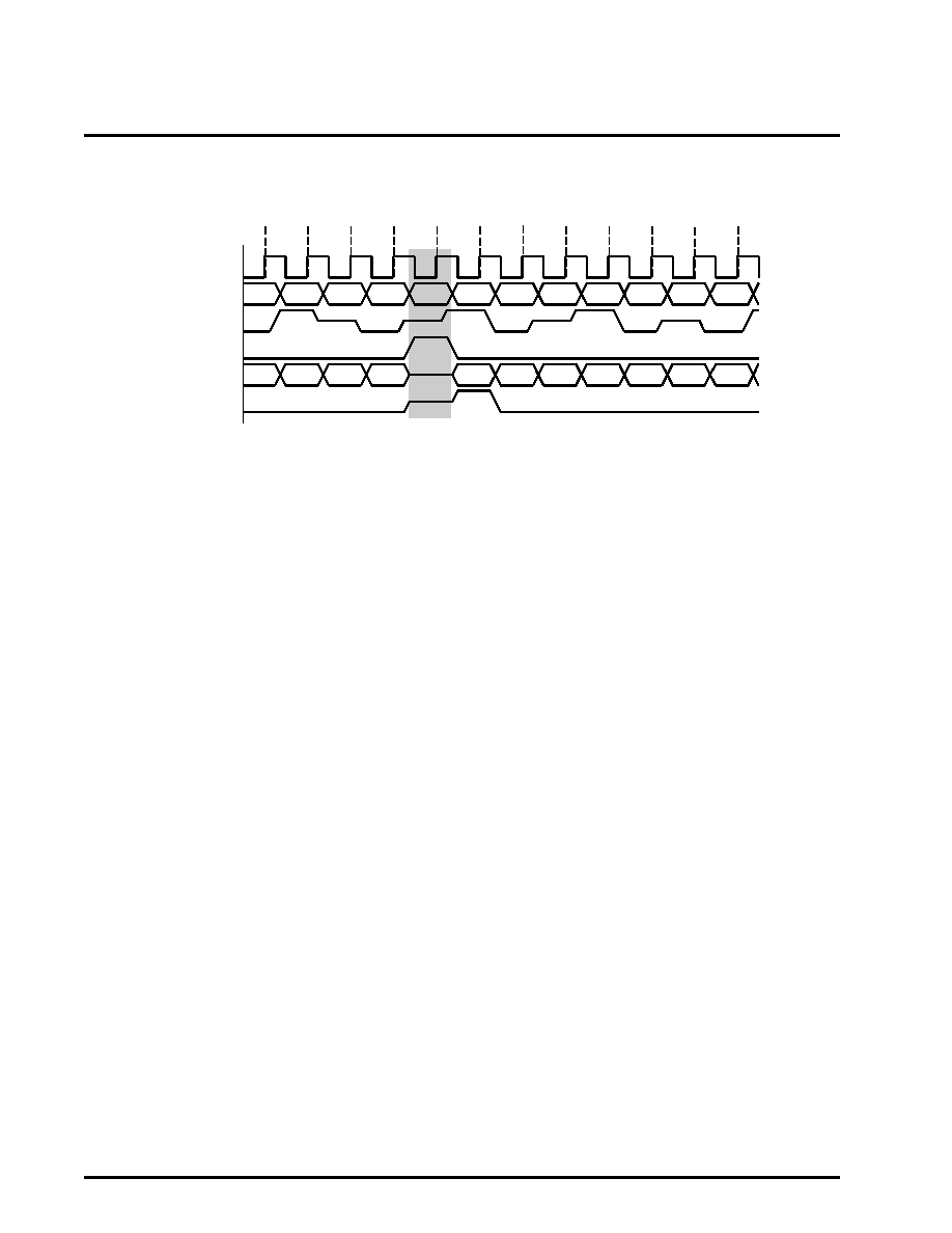
Figure 18: Timing Diagram of the Transmit UTOPIA Data and Address Bus signals, during the “Multi-
PHY” UNI Device Selection and Write Operations
TxUClk
TxUAddr[4:0]
TxUClav
TxUEnB*
TxUData[15:0]
TxUSoC
0x00
0x1F
0x02
0x1F
0x00
0x02
0x1F
0x00
0x02
0x1F
0x02
0x00
W0
W1
W2
W3
W4
W5
W6
W26
W25
W24
W23
Cell Transmitted to 0x02
Cell Transmitted to 0x00
0x00
0x02
0x00
0x02
0x00
0x02
1
2
3
4
5
6
7
8
9
10
11
12
Notes regarding Figure 18:
1. The Transmit UTOPIA Data bus is configured to be 16 bits wide. Hence, the data, which the ATM Layer
processor places on the Transmit UTOPIA Data bus, is expressed in terms of 16-bit words (e.g., W0 - W26).
2. The Transmit UTOPIA Interface Block is configured to handle 54 bytes/cell. Hence, Figure 29 illustrates
the ATM Layer processor writing 27 words (e.g., W0 through W26) for each ATM cell.
In Figure 29, the ATM Layer processor is initially writing ATM cell data to the Transmit UTOPIA Interface
block within UNI #2 (TxUAddr[4:0] = 0x02). However, the ATM Layer processor is also polling the Transmit
UTOPIA Interface block within UNI #1 (TxAddr[4:0] = 0x00) and the “NULL” address of 0x1F. The ATM Layer
processor completes its writing of the cell to UNI #1 at clock edge #4. Afterwards, the ATM Layer processor
will cease to write any more cell data to UNI #1, and will begin to write this data into UNI #2 (TxUAddr[4:0] =
0x02). The ATM Layer processor will indicate its intentions to select a new UNI device for writing by negating
the TxUEnB* signal, at clock edge #5 (see the shaded portion of Figure 29). At this time, UNI #1 will notice
two things:
1. The UTOPIA Address for the Transmit UTOPIA Interface block, within UNI #1 is on the Transmit UTOPIA
Address bus (TxUAddr[4:0] = 0x00).
2. The TxUEnB* signal has been negated.
UNI #1 will interpret this signaling as an indication that the ATM Layer processor is going to be performing
write operations to it. Afterwards, the ATM Layer processor will begin to write ATM cell data into Transmit
UTOPIA Interface block, within UNI #1.
2.2.1.4
UTOPIA LEVEL 3 OPERATION OF THE TRANSMIT UTOPIA INTERFACE BLOCK
BACK-TO-BACK POLLING
If the Transmit UTOPIA Interface block has been configured to operate in the UTOPIA Level 3 mode, then it
can be configured to support “Back-to-Back” polling.
UTOPIA Level 2 specifications mandate that the ATM Layer Processor interleave the application of UTOPIA
addresses with the “NULL” address of 0x1F.
If “Back-to-Back” polling is selected, then the ATM Layer Processor does not need to interleave the
application of UTOPIA addresses with the “NULL” address. Instead, the ATM Layer Processor can poll each
of the UNIs, by applying a different “UTOPIA Address” value, with each cycle of “TxUClk” (e.g., in a “Back-to-
Back” Manner).
The user can configure the “Transmit UTOPIA Interface” block to support “Back-to-Back” polling by setting bit
5 (Back-to-Back Polling Enable) within the “Transmit UTOPIA Control” Register, to “1” as depicted below.
相關PDF資料 |
PDF描述 |
|---|---|
| VI-B4J-IW-F1 | CONVERTER MOD DC/DC 36V 100W |
| 5413558-1 | CONN JACK BNC RT ANG 75 OHM GOLD |
| D38999/20WF32SN | CONN RCPT 32POS WALL MNT W/SCKT |
| D38999/20FF32SN | CONN RCPT 32POS WALL MNT W/SCKT |
| 5413515-2 | CONN JACK BNC RT ANG 50 OHM 30AU |
相關代理商/技術參數(shù) |
參數(shù)描述 |
|---|---|
| XRT94L33IB-F | 功能描述:網(wǎng)絡控制器與處理器 IC Demapper RoHS:否 制造商:Micrel 產品:Controller Area Network (CAN) 收發(fā)器數(shù)量: 數(shù)據(jù)速率: 電源電流(最大值):595 mA 最大工作溫度:+ 85 C 安裝風格:SMD/SMT 封裝 / 箱體:PBGA-400 封裝:Tray |
| XRT94L33IB-L | 功能描述:網(wǎng)絡控制器與處理器 IC Mapper / Demapper RoHS:否 制造商:Micrel 產品:Controller Area Network (CAN) 收發(fā)器數(shù)量: 數(shù)據(jù)速率: 電源電流(最大值):595 mA 最大工作溫度:+ 85 C 安裝風格:SMD/SMT 封裝 / 箱體:PBGA-400 封裝:Tray |
| XRT94L43 | 制造商:EXAR 制造商全稱:EXAR 功能描述:SONET/SDH STS-12/STM-4 TO E3/DS3/STS-1 MAPPER/DEMAPPER |
| XRT94L43_06 | 制造商:EXAR 制造商全稱:EXAR 功能描述:SONET/SDH OC-12 TO 12XDS3/E3 MAPPER |
| XRT94L43A | 制造商:EXAR 制造商全稱:EXAR 功能描述:SONET/SDH OC-12 TO 12XDS3/E3 MAPPER |
發(fā)布緊急采購,3分鐘左右您將得到回復。