- 您現(xiàn)在的位置:買賣IC網(wǎng) > PDF目錄1973 > XA3SD3400A-4FGG676I (Xilinx Inc)SPARTAN-3ADSP FPGA 3400K 676FBGA PDF資料下載
參數(shù)資料
| 型號(hào): | XA3SD3400A-4FGG676I |
| 廠商: | Xilinx Inc |
| 文件頁數(shù): | 33/58頁 |
| 文件大小: | 0K |
| 描述: | SPARTAN-3ADSP FPGA 3400K 676FBGA |
| 產(chǎn)品培訓(xùn)模塊: | Extended Spartan 3A FPGA Family |
| 標(biāo)準(zhǔn)包裝: | 40 |
| 系列: | Spartan®-3A DSP XA |
| LAB/CLB數(shù): | 5968 |
| 邏輯元件/單元數(shù): | 53712 |
| RAM 位總計(jì): | 2322432 |
| 輸入/輸出數(shù): | 469 |
| 門數(shù): | 3400000 |
| 電源電壓: | 1.14 V ~ 1.26 V |
| 安裝類型: | 表面貼裝 |
| 工作溫度: | -40°C ~ 100°C |
| 封裝/外殼: | 676-BGA |
| 供應(yīng)商設(shè)備封裝: | 676-FBGA(27x27) |
第1頁第2頁第3頁第4頁第5頁第6頁第7頁第8頁第9頁第10頁第11頁第12頁第13頁第14頁第15頁第16頁第17頁第18頁第19頁第20頁第21頁第22頁第23頁第24頁第25頁第26頁第27頁第28頁第29頁第30頁第31頁第32頁當(dāng)前第33頁第34頁第35頁第36頁第37頁第38頁第39頁第40頁第41頁第42頁第43頁第44頁第45頁第46頁第47頁第48頁第49頁第50頁第51頁第52頁第53頁第54頁第55頁第56頁第57頁第58頁
XA Spartan-3A DSP Automotive FPGA Family Data Sheet
DS705 (v2.0) April 18, 2011
Product Specification
39
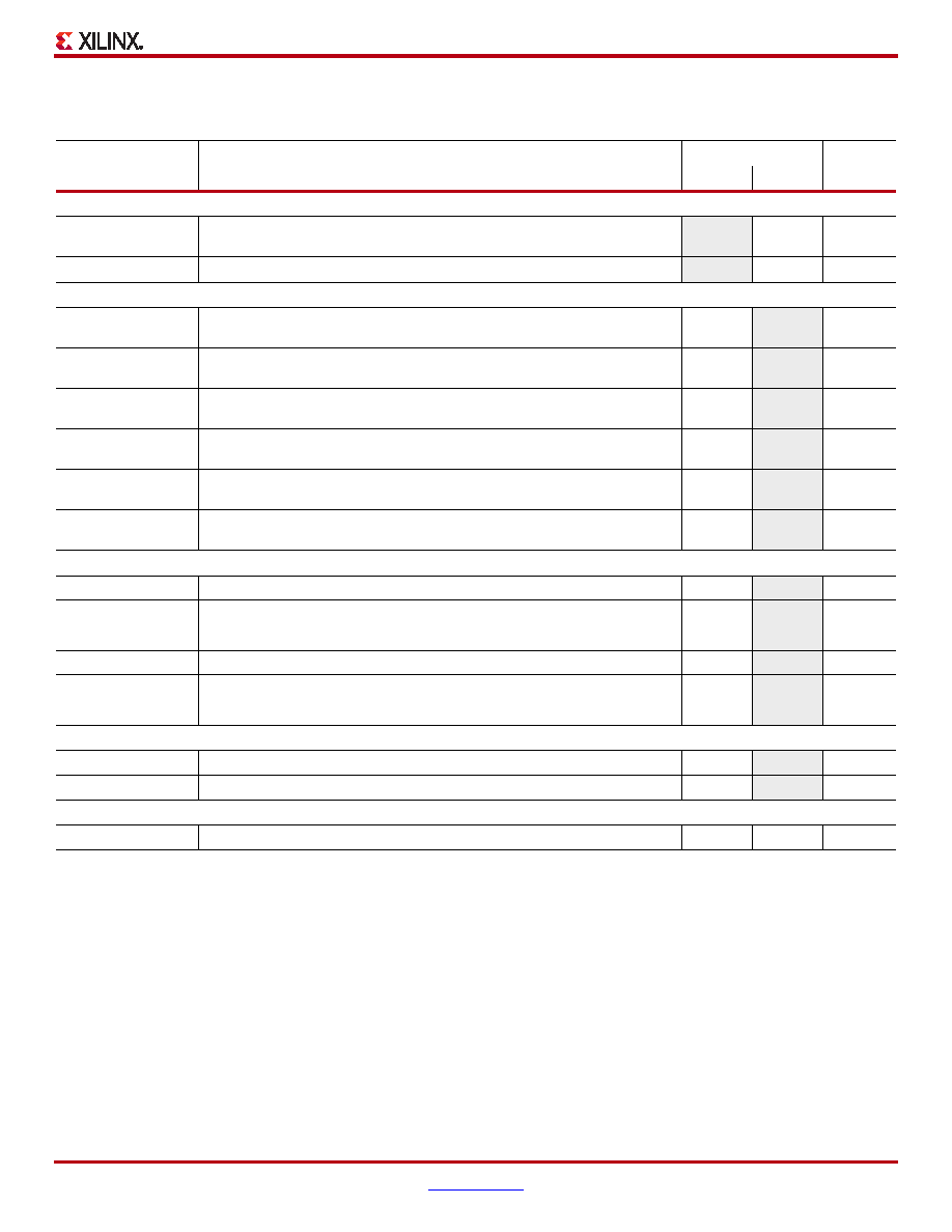
Block RAM Timing
Table 34: Block RAM Timing
Symbol
Description
Speed Grade: -4
Units
Min
Max
Clock-to-Output Times
TRCKO_DOA_NC
When reading from block RAM, the delay from the active transition at the CLK
input to data appearing at the DOUT output
–2.80
ns
TRCKO_DOA
Clock CLK to DOUT output (with output register)
–1.45
ns
Setup Times
TRCCK_ADDR
Setup time for the ADDR inputs before the active transition at the CLK input
of the block RAM
0.46
–ns
TRDCK_DIB
Setup time for data at the DIN inputs before the active transition at the CLK
input of the block RAM
0.33
–ns
TRCCK_ENB
Setup time for the EN input before the active transition at the CLK input of the
block RAM
0.60
–ns
TRCCK_WEB
Setup time for the WE input before the active transition at the CLK input of the
block RAM
0.75
–ns
TRCCK_REGCE
Setup time for the CE input before the active transition at the CLK input of the
block RAM
0.40
–ns
TRCCK_RST
Setup time for the RST input before the active transition at the CLK input of
the block RAM
0.25
–ns
Hold Times
TRCKC_ADDR
Hold time on the ADDR inputs after the active transition at the CLK input
0.10
–ns
TRDCK_DIB
Hold time on the DIN inputs after the active transition at the CLK input
0.10
–ns
TRCKC_ENB
Hold time on the EN input after the active transition at the CLK input
0.10
–ns
TRCKC_WEB
Hold time on the WE input after the active transition at the CLK input
0.10
–ns
TRCKC_REGCE
Hold time on the CE input after the active transition at the CLK input
0.10
–ns
TRCKC_RST
Hold time on the RST input after the active transition at the CLK input
0.10
–ns
Clock Timing
TBPWH
High pulse width of the CLK signal
1.79
–ns
TBPWL
Low pulse width of the CLK signal
1.79
–ns
Clock Frequency
FBRAM
Block RAM clock frequency
0
280
MHz
Notes:
1.
The numbers in this table are based on the operating conditions set forth in Table 8.
相關(guān)PDF資料 |
PDF描述 |
|---|---|
| XA6SLX75T-3FGG484Q | IC FPGA SPARTAN 6 484FGGBGA |
| XA95144XL-15CSG144I | IC CPLD 144MC 117 I/O 144CSBGA |
| XAM1808AZCE4 | IC ARM PROCESSOR 361NFBGA |
| XC1765ESOG8C | IC PROM SERIAL 65K 8-SOIC |
| XC17S200AVQ44I | IC PROM SER 200000 I-TEMP 44VQFP |
相關(guān)代理商/技術(shù)參數(shù) |
參數(shù)描述 |
|---|---|
| X-A4A-300L | 制造商:Leach International Corporation 功能描述:MID RANGE - Bulk |
| X-A4C-300M | 制造商:Leach International Corporation 功能描述:MID RANGE - Bulk |
| X-A4M-300L | 制造商:Leach International Corporation 功能描述:MID RANGE - Bulk |
| X-A4M-300M | 制造商:Leach International Corporation 功能描述:MID RANGE - Bulk |
| X-A4N | 制造商:Leach International Corporation 功能描述:MID RANGE - Bulk |
發(fā)布緊急采購,3分鐘左右您將得到回復(fù)。