- 您現(xiàn)在的位置:買賣IC網(wǎng) > PDF目錄202126 > W3H64M72E-667SBCF (WHITE ELECTRONIC DESIGNS CORP) 64M X 72 DDR DRAM, PBGA208 PDF資料下載
參數(shù)資料
| 型號(hào): | W3H64M72E-667SBCF |
| 廠商: | WHITE ELECTRONIC DESIGNS CORP |
| 元件分類: | DRAM |
| 英文描述: | 64M X 72 DDR DRAM, PBGA208 |
| 封裝: | 16 X 22 MM, 1 MM PITCH, LEAD FREE, PLASTIC, BGA-208 |
| 文件頁數(shù): | 10/32頁 |
| 文件大?。?/td> | 944K |
| 代理商: | W3H64M72E-667SBCF |
W3H64M72E-XSBX
W3H64M72E-XSBXF
18
White Electronic Designs Corporation (602) 437-1520 www.whiteedc.com
White Electronic Designs
December 2009
2010 White Electronic Designs Corp. All rights reserved
Rev. 9
White Electronic Designs Corp. reserves the right to change products or specications without notice.
READ COMMAND
The READ command is used to initiate a burst read access
to an active row. The value on the BA2–BA0 inputs selects
the bank, and the address provided on inputs A0–i (where
i = A9) selects the starting column location. The value on
input A10 determines whether or not auto precharge is
used. If auto precharge is selected, the row being accessed
will be precharged at the end of the READ burst; if auto
precharge is not selected, the row will remain open for
subsequent accesses.
READ OPERATION
READ bursts are initiated with a READ command. The
starting column and bank addresses are provided with the
READ command and auto precharge is either enabled or
disabled for that burst access. If auto precharge is enabled,
the row being accessed is automatically precharged at the
completion of the burst. If auto precharge is disabled, the
row will be left open after the completion of the burst.
During READ bursts, the valid data-out element from the
starting column address will be available READ latency
(RL) clocks later. RL is dened as the sum of AL and CL;
RL = AL + CL. The value for AL and CL are programmable
via the MR and EMR commands, respectively. Each
subsequent data-out element will be valid nominally at
the next positive or negative clock edge (i.e., at the next
crossing of CK and CK#).
DQS/DQS# is driven by the DDR2 SDRAM along with
output data. The initial LOW state on DQS and HIGH state
on DQS# is known as the read preamble (tRPRE). The
LOW state on DQS and HIGH state on DQS# coincident
with the last data-out element is known as the read
postamble (tRPST).
Upon completion of a burst, assuming no other commands
have been initiated, the DQ will go High-Z.
Data from any READ burst may be concatenated with
data from a subsequent READ command to provide a
continuous ow of data. The rst data element from the
new burst follows the last element of a completed burst.
The new READ command should be issued x cycles after
the rst READ command, where x equals BL / 2 cycles.
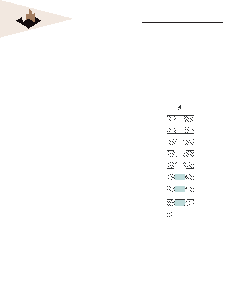
FIGURE 11 – READ COMMAND
DON’T CARE
CK
CK#
CS#
RAS#
CAS#
WE#
CKE
Col
Bank
ADDRESS
BANK ADDRESS
AUTO PRECHARGE
ENABLE
DISABLE
A10
相關(guān)PDF資料 |
PDF描述 |
|---|---|
| WS512K32-25G4C | 2M X 8 MULTI DEVICE SRAM MODULE, 25 ns, CQFP68 |
| WS1M8V-17CM | 1M X 8 STANDARD SRAM, 17 ns, CDIP32 |
| WS1M8V-20CC | 1M X 8 STANDARD SRAM, 20 ns, CDIP32 |
| WS1M8V-35CC | 1M X 8 STANDARD SRAM, 35 ns, CDIP32 |
| WS256K8-25CQE | 256K X 8 MULTI DEVICE SRAM MODULE, 25 ns, CDMA32 |
相關(guān)代理商/技術(shù)參數(shù) |
參數(shù)描述 |
|---|---|
| W3H64M72E-667SBI | 制造商:Microsemi Corporation 功能描述:64M X 72 DDR2, 1.8V, 667MHZ, 208PBGA INDUSTRIAL TEMP. - Bulk |
| W3H64M72E-667SBM | 制造商:Microsemi Corporation 功能描述:64M X 72 DDR2, 1.8V, 667MHZ, 208PBGA MIL-TEMP. - Bulk 制造商:Microsemi Corporation 功能描述:SDRAM MEMORY |
| W3H64M72EERXXXAD7MG | 制造商:WEDC 制造商全稱:White Electronic Designs Corporation 功能描述:512MB - 64Mx72 DDR2 SDRAM REGISTERED, w/PLL, VLP Mini-DIMM |
| W3H64M72EERXXXAD7SG | 制造商:WEDC 制造商全稱:White Electronic Designs Corporation 功能描述:512MB - 64Mx72 DDR2 SDRAM REGISTERED, w/PLL, VLP Mini-DIMM |
| W3H64M72E-ES | 制造商:WEDC 制造商全稱:White Electronic Designs Corporation 功能描述:64M x 72 DDR2 SDRAM 208 PBGA Multi-Chip Package |
發(fā)布緊急采購(gòu),3分鐘左右您將得到回復(fù)。