- 您現(xiàn)在的位置:買賣IC網(wǎng) > PDF目錄373631 > TFRA08C13 (Lineage Power) Ultraframer DS3/E3/DS2/E2/DS1/E1/DS0 PDF資料下載
參數(shù)資料
| 型號(hào): | TFRA08C13 |
| 廠商: | Lineage Power |
| 元件分類: | 通信及網(wǎng)絡(luò) |
| 英文描述: | Ultraframer DS3/E3/DS2/E2/DS1/E1/DS0 |
| 中文描述: | Ultraframer DS3/E3/DS2/E2/DS1/E1/DS0 |
| 文件頁數(shù): | 18/188頁 |
| 文件大小: | 3047K |
| 代理商: | TFRA08C13 |
第1頁第2頁第3頁第4頁第5頁第6頁第7頁第8頁第9頁第10頁第11頁第12頁第13頁第14頁第15頁第16頁第17頁當(dāng)前第18頁第19頁第20頁第21頁第22頁第23頁第24頁第25頁第26頁第27頁第28頁第29頁第30頁第31頁第32頁第33頁第34頁第35頁第36頁第37頁第38頁第39頁第40頁第41頁第42頁第43頁第44頁第45頁第46頁第47頁第48頁第49頁第50頁第51頁第52頁第53頁第54頁第55頁第56頁第57頁第58頁第59頁第60頁第61頁第62頁第63頁第64頁第65頁第66頁第67頁第68頁第69頁第70頁第71頁第72頁第73頁第74頁第75頁第76頁第77頁第78頁第79頁第80頁第81頁第82頁第83頁第84頁第85頁第86頁第87頁第88頁第89頁第90頁第91頁第92頁第93頁第94頁第95頁第96頁第97頁第98頁第99頁第100頁第101頁第102頁第103頁第104頁第105頁第106頁第107頁第108頁第109頁第110頁第111頁第112頁第113頁第114頁第115頁第116頁第117頁第118頁第119頁第120頁第121頁第122頁第123頁第124頁第125頁第126頁第127頁第128頁第129頁第130頁第131頁第132頁第133頁第134頁第135頁第136頁第137頁第138頁第139頁第140頁第141頁第142頁第143頁第144頁第145頁第146頁第147頁第148頁第149頁第150頁第151頁第152頁第153頁第154頁第155頁第156頁第157頁第158頁第159頁第160頁第161頁第162頁第163頁第164頁第165頁第166頁第167頁第168頁第169頁第170頁第171頁第172頁第173頁第174頁第175頁第176頁第177頁第178頁第179頁第180頁第181頁第182頁第183頁第184頁第185頁第186頁第187頁第188頁
Preliminary Data Sheet
October 2000
TFRA08C13 OCTAL T1/E1 Framer
18
L Lucent Technologies Inc.
Pin Information
(continued)
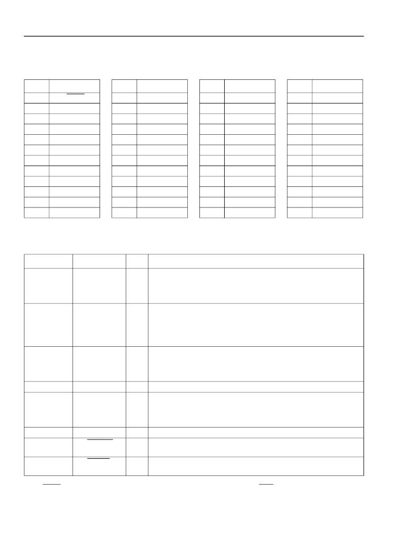
Table 1. Pin Assignments for 352-Pin PBGA by Pin Number Order
(continued)
Table 2 shows the list of the TFRA08C13 pins and a functional description for each.
Table 2. Pin Descriptions
Pin
Signal Name
Pin
Signal Name
Pin
Signal Name
Pin
Signal Name
AE5
AE6
AE7
AE8
AE9
AE10
AE11
AE12
AE13
AE14
AE15
AE16
DS1/CEPT3
A2
A6
A9
SECOND
MPCLK
RCHIDATAB4
TFDLCK4
TFS4
AD1
AD5
AD7
AE17
AE18
AE19
AE20
AE21
AE22
AE23
AE24
AE25
AE26
AF1
AF2
RFDLCK4
RFRMDATA4
NC
TND4
V
SS
TPD5
NC
NC
NC
TLCK5
NC
RFRMCLK3
AF3
AF4
AF5
AF6
AF7
AF8
AF9
AF10
AF11
AF12
AF13
AF14
V
DD
RLCK3
V
DD
A5
A7
A11
MPMODE
RPD4
TFDL4
TCRCMFS4
TCHIDATA4
AD3
AF15
AF16
AF17
AF18
AF19
AF20
AF21
AF22
AF23
AF24
AF25
AF26
AD6
NC
RSSFS4
NC
TLCK4
RLCK4
RLCK5
TND5
NC
NC
NC
NC
Pins
Symbol
Type
*
Description
AF3, AF5,
AD18, K25,
E24, K4,
M2, U3
AD20, AD26,
AE21, G3,
K24,
A18, J3, C7,
Y2
D17
V
DD
P
3.3 V Power Supply.
3.3 V ± 5%. Each of these pins must be bypassed
with a 0.1
μ
F capacitor to V
SS
, as close to the pin as possible.
V
SS
G
Ground.
V
DDA
P
3.3 V Quiet Analog Power Supply.
This pin must be bypassed with a
0.1
μ
F capacitor to V
SSA
, as close to the pin as possible. In addition,
this pin should be isolated from the 3.3 V power plane with an inductive
bead.
3.3 V Quiet Analog Ground.
3.3 V Quiet Digital Power Supply.
This pin must be bypassed with a
0.1
μ
F capacitor to V
SSD
, as close to the pin as possible. In addition,
this pin should be isolated from the 3.3 V power plane with an inductive
bead.
3.3 V Quiet Digital Ground.
3-State (Active-Low).
Asserting this pin low forces the channel outputs
into a high-impedance state.
Reset (Active-Low).
Asserting this pin low resets all channels on the
entire device.
C17
A14
V
SSA
V
DDD
G
P
A13
B18
V
SSD
3-STATE
G
I
u
C19
RESET
I
u
* I
u
indicates an internal pull-up, I
d
indicates an internal pull-down.
After RESET is deasserted, the channel is in the default framing mode, as a function of the DS1/CEPT pin.
Asserting this pin low will initially force RDY to a low state.
相關(guān)PDF資料 |
PDF描述 |
|---|---|
| TFS380C | VI TELEFILTER Filter specification |
| TFT0675F | Anti-Aliasing and Reconstruction TFT range |
| TFT0675S | Anti-Aliasing and Reconstruction TFT range |
| TFT1350F | Anti-Aliasing and Reconstruction TFT range |
| TFT1350S | Anti-Aliasing and Reconstruction TFT range |
相關(guān)代理商/技術(shù)參數(shù) |
參數(shù)描述 |
|---|---|
| TFRA08C13-DB | 制造商:AGERE 制造商全稱:AGERE 功能描述:TFRA08C13 OCTAL T1/E1 Framer |
| TFRA28J133BAL-1 | 制造商:未知廠家 制造商全稱:未知廠家 功能描述:Telecomm/Datacomm |
| TFRA84J13 | 制造商:AGERE 制造商全稱:AGERE 功能描述:Ultraframer DS3/E3/DS2/E2/DS1/E1/DS0 |
| TFRA84J131BL-3-DB | 制造商:LSI Corporation 功能描述:Framer DS0/DS1/DS2/DS3/E1/E2/E3 1.5V/3.3V 909-Pin BGA |
| TFRA84J13DS0 | 制造商:AGERE 制造商全稱:AGERE 功能描述:Ultraframer DS3/E3/DS2/E2/DS1/E1/DS0 |
發(fā)布緊急采購,3分鐘左右您將得到回復(fù)。