- 您現(xiàn)在的位置:買賣IC網 > PDF目錄379343 > SAF7849HL (NXP Semiconductors N.V.) One chip CD audio device with integrated MP3-WMA decoder PDF資料下載
參數(shù)資料
| 型號: | SAF7849HL |
| 廠商: | NXP Semiconductors N.V. |
| 元件分類: | 存儲器 |
| 英文描述: | One chip CD audio device with integrated MP3-WMA decoder |
| 封裝: | SAF7843HL/M295<SOT486-1 (LQFP144)|<<http://www.nxp.com/packages/SOT486-1.html<1<Always Pb-free,;SAF7849HL/M245<SOT486-1 (LQFP144)|<<http://www.nxp.com/packages/SOT486-1.h |
| 文件頁數(shù): | 25/93頁 |
| 文件大小: | 396K |
| 代理商: | SAF7849HL |
第1頁第2頁第3頁第4頁第5頁第6頁第7頁第8頁第9頁第10頁第11頁第12頁第13頁第14頁第15頁第16頁第17頁第18頁第19頁第20頁第21頁第22頁第23頁第24頁當前第25頁第26頁第27頁第28頁第29頁第30頁第31頁第32頁第33頁第34頁第35頁第36頁第37頁第38頁第39頁第40頁第41頁第42頁第43頁第44頁第45頁第46頁第47頁第48頁第49頁第50頁第51頁第52頁第53頁第54頁第55頁第56頁第57頁第58頁第59頁第60頁第61頁第62頁第63頁第64頁第65頁第66頁第67頁第68頁第69頁第70頁第71頁第72頁第73頁第74頁第75頁第76頁第77頁第78頁第79頁第80頁第81頁第82頁第83頁第84頁第85頁第86頁第87頁第88頁第89頁第90頁第91頁第92頁第93頁
SAF784X_2
NXP B.V. 2008. All rights reserved.
Product data sheet
Rev. 02 — 9 May 2008
25 of 93
NXP Semiconductors
SAF784x
One chip CD audio device with integrated MP3/WMA decoder
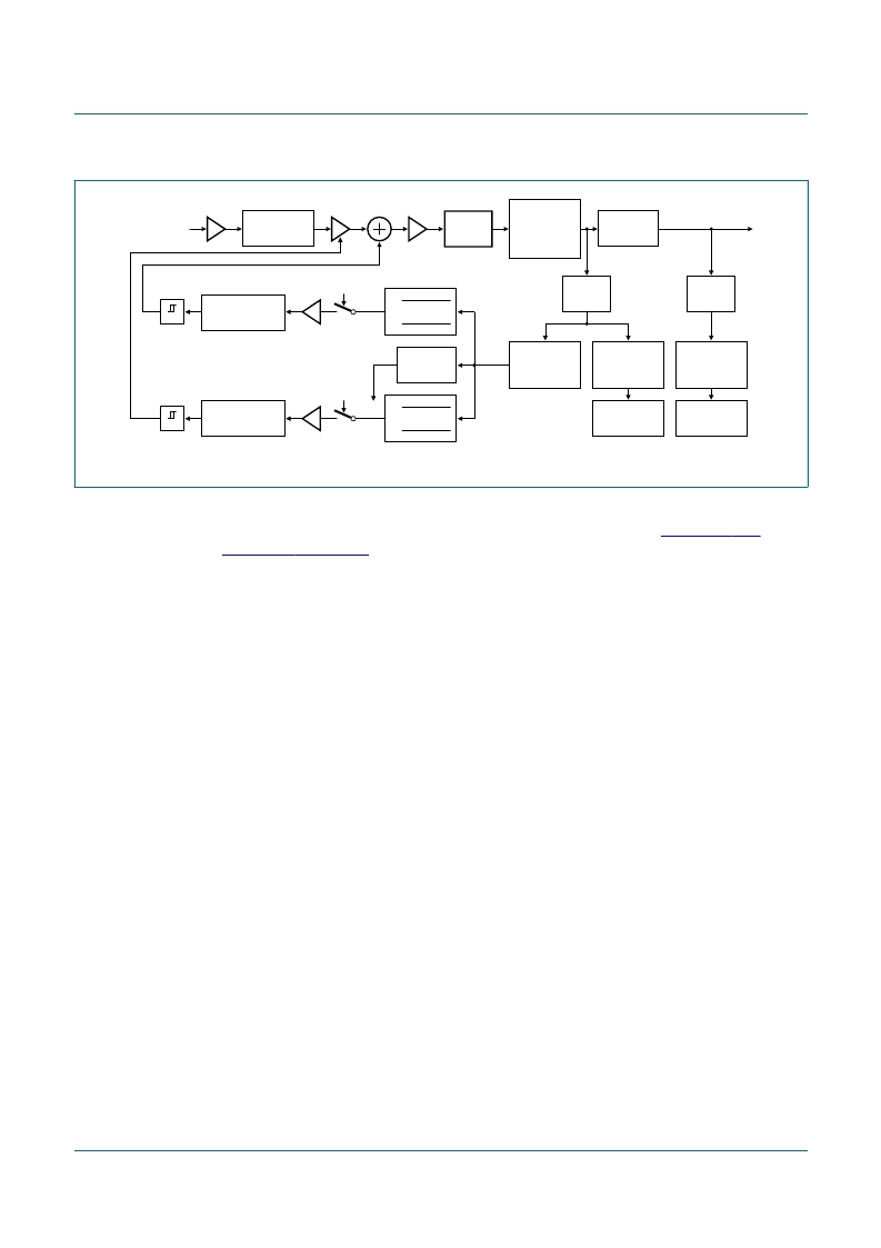
The maximum and minimum peaks on the envelope of the RF signal after the ADC are
first measured via a noise filter and the window peak detector (see
Section “Peak
Detectors” on page 23
. The amplitude is then calculated as maxpeak
minpeak, and the
offset as (maxpeak + minpeak) / 2.
For tuning the loops, it is possible to read back the HFMaxPeak, HFMinPeak,
HFAmplitude and HFOffset, as measured from their registers by the decay peak detector.
AGC control:
The RF amplitude at the ADC input can be changed with two gain
amplifiers in the analog part: G1 (fixed) and G2 (dynamic). G1 has a gain range from 0 dB
to 24 dB in 16 steps of 1.6 dB, while G2 has a range from 0 dB to 12 dB in 16 steps of 0.8
dB. Both gains can be programmed via register AGCGain. G1 will stay fixed, while G2 can
be regulated by hardware when the AGC is turned on.
The AGC will regulate the gain such that the measured amplitude stays between a
programmed upper threshold (AGCThrHi) and lower threshold (AGCThrLo). If the
amplitude is smaller, gain will increase; if the amplitude is too large, gain will decrease.
When clipping is detected on either one or both sides, the gain will decrease. These gain
changes are not sent to the analog gain amplifier directly but are integrated over time.
Only if, on average, a gain increase or decrease is requested, will this result in a real gain
increase or decrease of the amplifier. This can also be read back via register AGCGain.
The AGC, together with the noise filter on the peak detector, prevents RF noise causing
over-sensitive gain regulation. To further reduce sensitive behavior, a hysteresis window
with a width of one gain step is added between the integrator and amplifier G2. The
bandwidth of the gain loop determines how fast it reacts to fingerprints and scratches; it is
programmed via register AGCIntegBW. It is also possible to limit the range of G2 by
programming a maximum and minimum boundary by register AGCGainBound.
AOC control:
Most of the RF offset at the ADC input will be removed by the analog HPF
(1st-order HPF with 3 dB point around 3.6 kHz). The remaining offset (mainly introduced
by the analog front end), can be removed by adding or subtracting a fixed offset in the
analog part. This offset subtraction/addition has a range of 32 steps in each direction, with
approximately 1.4 LSBs per step (referenced to the RF ADC). This leads to a full
Fig 14. AGC and AOC loops
001aag318
HPF
(DIGITAL)
6 MSBs
K gain
software/
defect
INTEGRATOR
lo
hi
1
+1
1
+1
to bit detection
G1
G2
G3
HPF
ANALOG
DEFECT
DETECT
REGISTERS
INTEGRATOR
CLIPPING
DETECT
DECAY
PEAK
DETECTOR
WINDOW
PEAK
DETECTOR
DECAY
PEAK
DETECTOR
INTEGRATE
AND
DUMP
FILTER
NF
(LPF)
NF
(LPF)
ADC
K offset
software/
defect
lo
hi
4 MSBs
相關PDF資料 |
PDF描述 |
|---|---|
| SB-015 | GMR Digital Sensor Evaluation Kit |
| SB10100F | ISOLATION SCHOTTKY BARRIER RECTIFIERS |
| SB1040F | ISOLATION SCHOTTKY BARRIER RECTIFIERS |
| SB1080F | ISOLATION SCHOTTKY BARRIER RECTIFIERS |
| SB1020F | ISOLATION SCHOTTKY BARRIER RECTIFIERS |
相關代理商/技術參數(shù) |
參數(shù)描述 |
|---|---|
| SAF7849HL/M245,557 | 功能描述:音頻 DSP IC AUD DECODER RoHS:否 制造商:Texas Instruments 工作電源電壓: 電源電流: 工作溫度范圍: 安裝風格: 封裝 / 箱體: 封裝:Tube |
| SAF7849HL/M295,557 | 功能描述:音頻 DSP IC AUD DECODER RoHS:否 制造商:Texas Instruments 工作電源電壓: 電源電流: 工作溫度范圍: 安裝風格: 封裝 / 箱體: 封裝:Tube |
| SAF7860HL/M2,557 | 制造商:NXP Semiconductors 功能描述:DSP |
| SAF82520PVB2 | 制造商:SIEMENS 功能描述:New |
| SAF82525 | 制造商:INFINEON 制造商全稱:Infineon Technologies AG 功能描述:Data Communications ICs |
發(fā)布緊急采購,3分鐘左右您將得到回復。