- 您現(xiàn)在的位置:買賣IC網(wǎng) > PDF目錄379343 > SAF7846HL (NXP Semiconductors N.V.) One chip CD audio device with integrated MP3-WMA decoder PDF資料下載
參數(shù)資料
| 型號: | SAF7846HL |
| 廠商: | NXP Semiconductors N.V. |
| 元件分類: | 存儲器 |
| 英文描述: | One chip CD audio device with integrated MP3-WMA decoder |
| 封裝: | SAF7843HL/M295<SOT486-1 (LQFP144)|<<http://www.nxp.com/packages/SOT486-1.html<1<Always Pb-free,;SAF7849HL/M245<SOT486-1 (LQFP144)|<<http://www.nxp.com/packages/SOT486-1.h |
| 文件頁數(shù): | 21/93頁 |
| 文件大小: | 396K |
| 代理商: | SAF7846HL |
第1頁第2頁第3頁第4頁第5頁第6頁第7頁第8頁第9頁第10頁第11頁第12頁第13頁第14頁第15頁第16頁第17頁第18頁第19頁第20頁當前第21頁第22頁第23頁第24頁第25頁第26頁第27頁第28頁第29頁第30頁第31頁第32頁第33頁第34頁第35頁第36頁第37頁第38頁第39頁第40頁第41頁第42頁第43頁第44頁第45頁第46頁第47頁第48頁第49頁第50頁第51頁第52頁第53頁第54頁第55頁第56頁第57頁第58頁第59頁第60頁第61頁第62頁第63頁第64頁第65頁第66頁第67頁第68頁第69頁第70頁第71頁第72頁第73頁第74頁第75頁第76頁第77頁第78頁第79頁第80頁第81頁第82頁第83頁第84頁第85頁第86頁第87頁第88頁第89頁第90頁第91頁第92頁第93頁
SAF784X_2
NXP B.V. 2008. All rights reserved.
Product data sheet
Rev. 02 — 9 May 2008
21 of 93
NXP Semiconductors
SAF784x
One chip CD audio device with integrated MP3/WMA decoder
For the application, it should be noted that the interface supports 32-bit registers, while the
decoder only contains 8-bit registers. Therefore, the decoder registers are treated as
32-bit registers of which the 24 MSBs are not used.
The register address map occupied by the decoder goes from relative address
0x3000 0000 to address 0x3000 0374, and can be split into two parts:
0x3000 0000 - 0x3000 024C: the decoder’s own registers - used to configure the
channel decoder, and the functionality they control is described in detail in this section.
0x3000 02A0 - 0x3000 0374: the decoder immigrant registers - used to control parts of
the SAF784x that do not have their own AHB interface (they are not used to control the
decoder channel decoder).
6.5.4.2
Interrupt strategy
The channel decoder contains two interrupt status registers: InterruptStatus1 contains all
interrupts that operate as set/reset latches (set by hardware, reset by reading from the
register). InterruptStatus2 contains all interrupts that operate as feed-throughs (set by
hardware, reset by hardware or by accessing other registers).
Each interrupt bit can be enabled or disabled separately by writing to its corresponding
enable bit in the InterruptEnable1 and InterruptEnable2 registers. If one or several
interrupt bits are set and at least one is enabled, the interrupt line of the decoder to the
microcontroller will go active (LOW). If an interrupt bit is disabled (enable bit turned off), it
is prevented from activating the interrupt line to the microcontroller. However, this mode
allows the interrupt to be processed if the status register is polled instead of interrupt
handling by the microcontroller.
6.5.5
EFM bit detection and demodulation
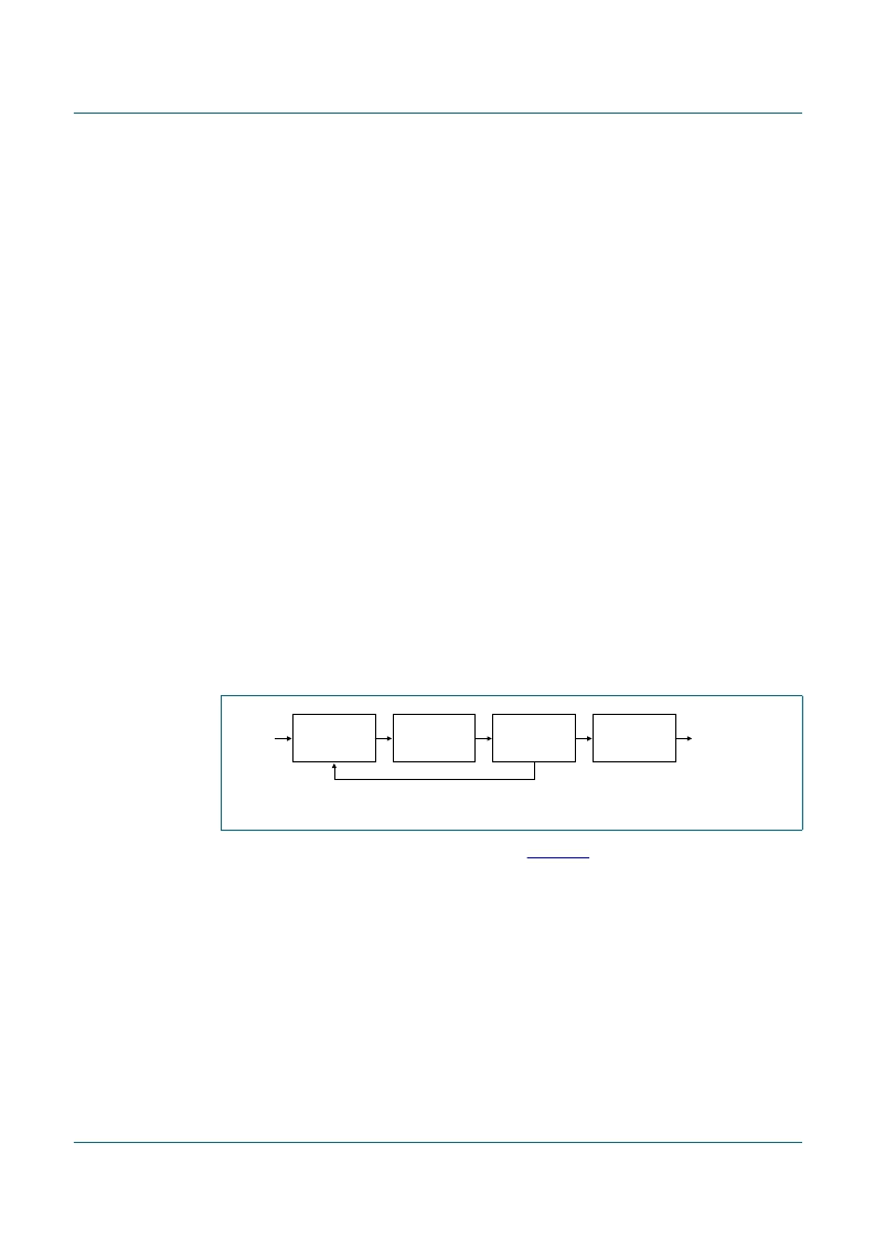
A block diagram of the bit recovery is shown in
Figure 10
.
The HF signal comprises the four diode inputs inside the analog block. It is pre-processed
(LPF, HPF, offset removal and gain adjustment) and then sampled by a 6-bit ADC.
On the sampled HF, bit recovery is done by means of a full digital PLL and slicer.
Before the sampled signal enters the PLL section, it is pre-processed by a signal
conditioning block. This consists of an integrate-and-dump block, a high-pass filter and
logic available for gain control and offset control on the RF signal in the analog section.
For good playability on defects, a defect detector puts the PLL, the slicer, the AGC, the
offset cancellation and the high-pass filter into hold during defects.
Fig 10. Bit recovery block diagram
001aag314
D1
D2
D3
D4
to demodulator
AGC
AOC
SIGNAL
CONDITIONING
BLOCK
6-bit
ADC
ANALOG
BLOCK
PLL AND
BIT SLICER
相關PDF資料 |
PDF描述 |
|---|---|
| SAF7847HL | One chip CD audio device with integrated MP3-WMA decoder |
| SAF7849HL | One chip CD audio device with integrated MP3-WMA decoder |
| SB-015 | GMR Digital Sensor Evaluation Kit |
| SB10100F | ISOLATION SCHOTTKY BARRIER RECTIFIERS |
| SB1040F | ISOLATION SCHOTTKY BARRIER RECTIFIERS |
相關代理商/技術參數(shù) |
參數(shù)描述 |
|---|---|
| SAF7846HL/M210,557 | 功能描述:音頻 DSP 1 chip CD Audio Dev w/Integrated decoder RoHS:否 制造商:Texas Instruments 工作電源電壓: 電源電流: 工作溫度范圍: 安裝風格: 封裝 / 箱體: 封裝:Tube |
| SAF7847HL/M201,557 | 功能描述:音頻 DSP 1 chip CD Audio Dev w/Integrated decoder RoHS:否 制造商:Texas Instruments 工作電源電壓: 電源電流: 工作溫度范圍: 安裝風格: 封裝 / 箱體: 封裝:Tube |
| SAF7849HL/M245,557 | 功能描述:音頻 DSP IC AUD DECODER RoHS:否 制造商:Texas Instruments 工作電源電壓: 電源電流: 工作溫度范圍: 安裝風格: 封裝 / 箱體: 封裝:Tube |
| SAF7849HL/M295,557 | 功能描述:音頻 DSP IC AUD DECODER RoHS:否 制造商:Texas Instruments 工作電源電壓: 電源電流: 工作溫度范圍: 安裝風格: 封裝 / 箱體: 封裝:Tube |
| SAF7860HL/M2,557 | 制造商:NXP Semiconductors 功能描述:DSP |
發(fā)布緊急采購,3分鐘左右您將得到回復。