- 您現(xiàn)在的位置:買賣IC網(wǎng) > PDF目錄367816 > PCF50732H (NXP SEMICONDUCTORS) Baseband and audio interface for GSM PDF資料下載
參數(shù)資料
| 型號: | PCF50732H |
| 廠商: | NXP SEMICONDUCTORS |
| 元件分類: | 通信及網(wǎng)絡(luò) |
| 英文描述: | Baseband and audio interface for GSM |
| 中文描述: | SPECIALTY TELECOM CIRCUIT, PQFP48 |
| 封裝: | PLASTIC, LQFP-48 |
| 文件頁數(shù): | 13/64頁 |
| 文件大小: | 322K |
| 代理商: | PCF50732H |
第1頁第2頁第3頁第4頁第5頁第6頁第7頁第8頁第9頁第10頁第11頁第12頁當前第13頁第14頁第15頁第16頁第17頁第18頁第19頁第20頁第21頁第22頁第23頁第24頁第25頁第26頁第27頁第28頁第29頁第30頁第31頁第32頁第33頁第34頁第35頁第36頁第37頁第38頁第39頁第40頁第41頁第42頁第43頁第44頁第45頁第46頁第47頁第48頁第49頁第50頁第51頁第52頁第53頁第54頁第55頁第56頁第57頁第58頁第59頁第60頁第61頁第62頁第63頁第64頁
1999 May 03
13
Philips Semiconductors
Objective specification
Baseband and audio interface for GSM
PCF50732
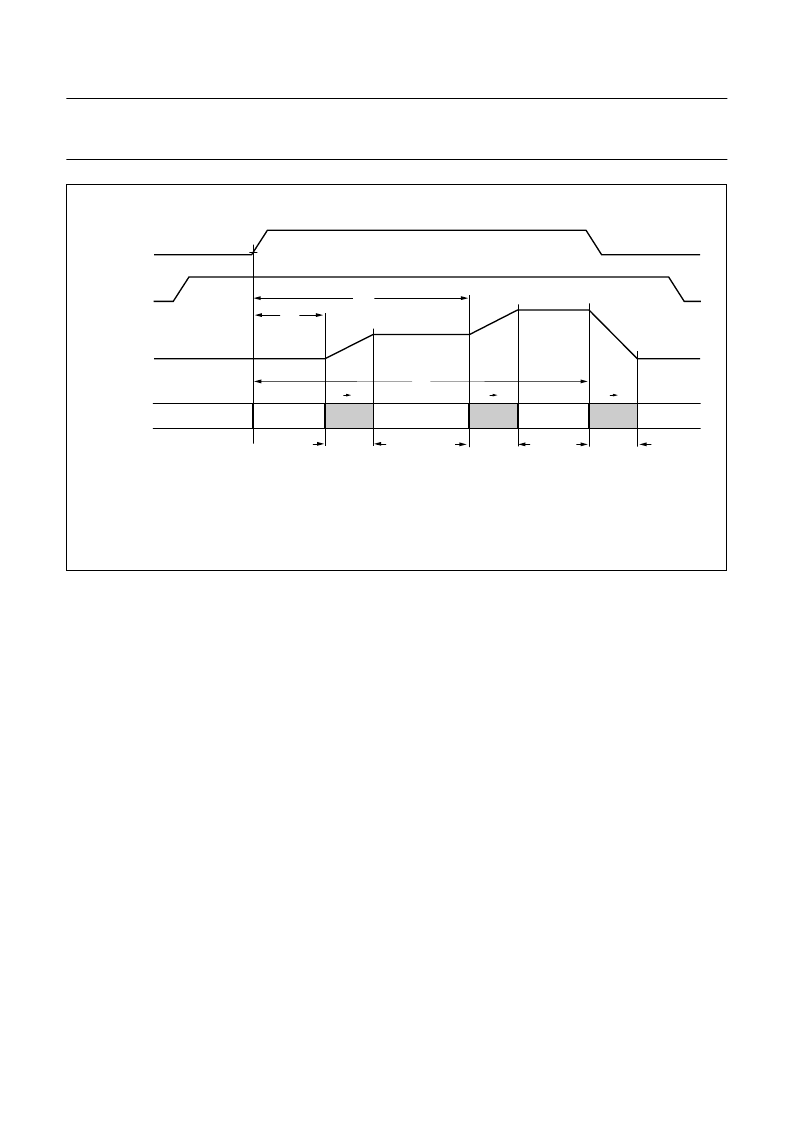
Fig.4 Power ramping timing characteristics (multislot mode).
(1) APE_DAC3: Analog Power Enable signal for the AUXDAC3.
handbook, full pagewidth
MGR995
trup
trim
trdo
RU
RM
RD
tru
AUXDAC3
TXON
APE_DAC3
(1)
ADDRESS
AUXDAC3
RAM
0 15
15 31
31
47
15
47
47
31 47
tim
trd
9.3.3
R
ECEIVER PATH BLOCK DESCRIPTION
9.3.3.1
Receive serial interface
The baseband serial interface sends the digital signal of
the receive path to a digital signal processor. It also takes
the digital bitstream from the digital signal processor and
transmits it via the baseband CODEC.
The baseband reception and transmission are active in
bursts. A normal burst has a length of 548
μ
s. The frame
rate of bursts is 4.615 ms. Using a normal traffic channel,
one burst for each frame is transmitted and two bursts are
received. To save as much power as possible, the transmit
path and the receive path of the PCF50732 are in
power-up mode only during the transmission or reception
bursts respectively.
The power-up of the receive section is controlled via the
RXON pin or RXON bit. When RXON is driven HIGH, the
receive section recovers from power-down and the output
clock BIOCLK is activated. After a settling delay of 52
μ
s
(ZIF mode, analog circuitry + decimation filter settling
time), BOEN goes LOW to transfer the first 12-bit
I and Q words. The settling time is only 26
μ
s in NZIF
mode.
Bits are clocked out of the PCF50732 by the falling edge,
and clocked into the DSP by the rising edge of BIOCLK.
In normal bursts 148 I/Q pairs are read from the
PCF50732.
When RXON goes LOW, the last pair of I and Q values will
be sampled and transferred to the baseband processor
(both I and Q components). BIOCLK stops after additional
16 BIOCLK cycles. The receive path is powered down
again. In power-down the BIOCLK output is put in 3-state
and the BOEN output is HIGH.
The output format is 2
×
12-bit I/Q (twos complement).
Transmission occurs MSB first, I followed by Q. The serial
clock signal BIOCLK will run at 6.5 MHz, or 13 MHz in the
NZIF mode. Figure 6 shows the timing of the BSI data
reception.
An automatic offset compensation mechanism is provided
in order to achieve the required performance. This
mechanism will short the receive (RX) inputs internally and
measure the resulting offset value. This offset value will be
subtracted from all subsequent I/Q output words.
The offset inherent to the device can thereby be reduced
to a few millivolts. Default value for both I- and Q-offset is
zero.
相關(guān)PDF資料 |
PDF描述 |
|---|---|
| PCF7991AT | Advanced Basestation IC, ABIC |
| PCF80C31BH4-24H | CMOS single-chip 8-bit microcontrollers |
| PCB80C51BH-2H | CMOS single-chip 8-bit microcontrollers |
| PCB80C51BH-2P | CMOS single-chip 8-bit microcontrollers |
| PCB80C51BH-2WP | CMOS single-chip 8-bit microcontrollers |
相關(guān)代理商/技術(shù)參數(shù) |
參數(shù)描述 |
|---|---|
| PCF5075 | 制造商:未知廠家 制造商全稱:未知廠家 功能描述:Power Control/Management |
| PCF5075TDK-T | 制造商:未知廠家 制造商全稱:未知廠家 功能描述:Power Control/Management |
| PCF5077T | 制造商:PHILIPS 制造商全稱:NXP Semiconductors 功能描述:Power amplifier controller for GSM and PCN systems |
| PCF5078 | 制造商:PHILIPS 制造商全稱:NXP Semiconductors 功能描述:Power amplifier controller for GSM and PCN systems |
| PCF5078T | 制造商:PHILIPS 制造商全稱:NXP Semiconductors 功能描述:Power amplifier controller for GSM and PCN systems |
發(fā)布緊急采購,3分鐘左右您將得到回復。