- 您現(xiàn)在的位置:買賣IC網(wǎng) > PDF目錄69026 > MC68HC05JB3JDW (MOTOROLA INC) 8-BIT, MROM, 3 MHz, MICROCONTROLLER, PDSO28 PDF資料下載
參數(shù)資料
| 型號: | MC68HC05JB3JDW |
| 廠商: | MOTOROLA INC |
| 元件分類: | 微控制器/微處理器 |
| 英文描述: | 8-BIT, MROM, 3 MHz, MICROCONTROLLER, PDSO28 |
| 封裝: | SOIC-28 |
| 文件頁數(shù): | 125/148頁 |
| 文件大小: | 1600K |
| 代理商: | MC68HC05JB3JDW |
第1頁第2頁第3頁第4頁第5頁第6頁第7頁第8頁第9頁第10頁第11頁第12頁第13頁第14頁第15頁第16頁第17頁第18頁第19頁第20頁第21頁第22頁第23頁第24頁第25頁第26頁第27頁第28頁第29頁第30頁第31頁第32頁第33頁第34頁第35頁第36頁第37頁第38頁第39頁第40頁第41頁第42頁第43頁第44頁第45頁第46頁第47頁第48頁第49頁第50頁第51頁第52頁第53頁第54頁第55頁第56頁第57頁第58頁第59頁第60頁第61頁第62頁第63頁第64頁第65頁第66頁第67頁第68頁第69頁第70頁第71頁第72頁第73頁第74頁第75頁第76頁第77頁第78頁第79頁第80頁第81頁第82頁第83頁第84頁第85頁第86頁第87頁第88頁第89頁第90頁第91頁第92頁第93頁第94頁第95頁第96頁第97頁第98頁第99頁第100頁第101頁第102頁第103頁第104頁第105頁第106頁第107頁第108頁第109頁第110頁第111頁第112頁第113頁第114頁第115頁第116頁第117頁第118頁第119頁第120頁第121頁第122頁第123頁第124頁當(dāng)前第125頁第126頁第127頁第128頁第129頁第130頁第131頁第132頁第133頁第134頁第135頁第136頁第137頁第138頁第139頁第140頁第141頁第142頁第143頁第144頁第145頁第146頁第147頁第148頁
GENERAL RELEASE SPECIFICATION
November 5, 1998
MOTOROLA
UNIVERSAL SERIAL BUS MODULE
MC68HC05JB3
10-10
REV 1
When using the remote wake-up capability, the rmware must wait for at least 5
ms after the bus is in the idle state before sending the remote wake-up resume
signaling. This allows the upstream devices to get into their suspend state and
prepare for propagating resume signaling. The FRESUM bit should be asserted to
cause the resume state on the USB data lines for at least 10ms, but not more than
15ms. Note that the resume signalling is controlled by the FRESUM bit and
meeting the timing specications is dependent on the rmware. When FRESUM is
cleared by rmware, the data lines will return to their high impedance state. Refer
to Section 10.5.5 for more information about how the Force Resume (FRESUM)
bit can be used to initiate the remote wake-up feature.
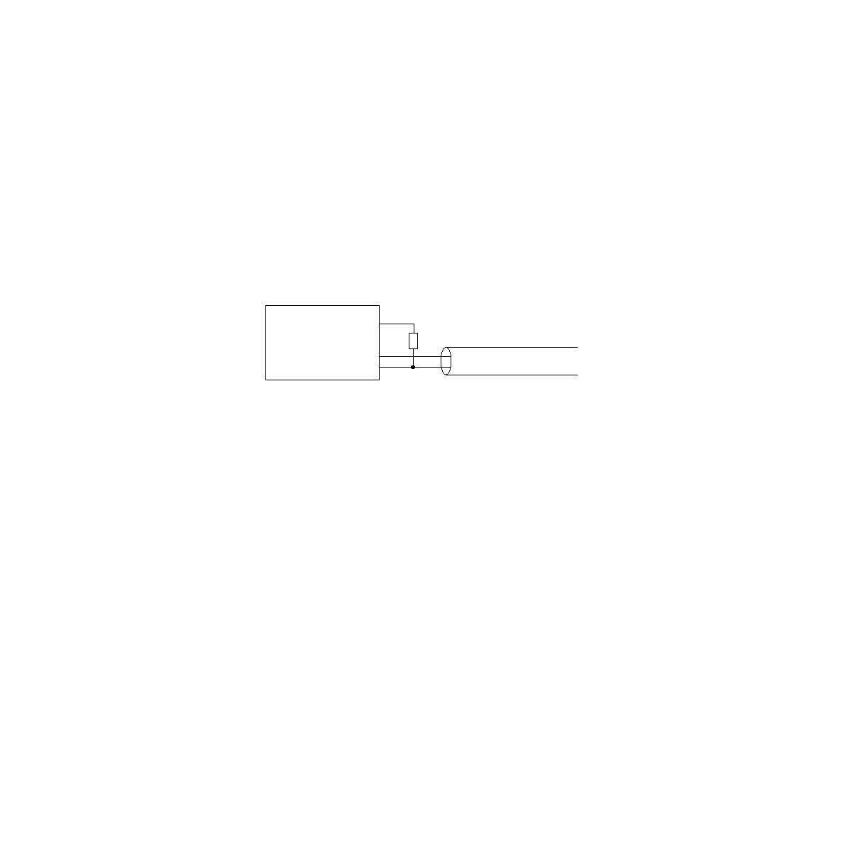
10.2.5 Low Speed Device
Externally, low speed devices are congured by the position of a pull-up resistor
on the USB D– pin of the MC68HC05JB3. Low speed devices are terminated as
shown in Figure 10-10 with the pull-up on the D– line.
Figure 10-10. External Low Speed Device Conguration
For low speed transmissions, the transmitter’s EOP width must be between
1.25
s and 1.50s. These ranges include timing variations due to differential
buffer delay and rise/fall time mismatches and to noise and other random effects.
A low speed receiver must accept a 670ns wide SE0 followed by a J transition as
a valid EOP. An SE0 narrower than 330ns or an SE0 not followed by a J transition
must be rejected as an EOP. An EOP between 330ns and 670ns may be rejected
or accepted as above. Any SE0 that is 2.5
s or wider is automatically a reset.
10.3
CLOCK REQUIREMENTS
The low speed data rate is nominally 1.5 Mbs. The OSCXCLK signal driven by the
oscillator circuits is the clock source for the USB module and requires that a 6
MHz oscillator circuit be connected to the OSC1 and OSC2 pins. The permitted
frequency tolerance for low speed functions is approximately
±1.5% (15000 ppm).
This tolerance includes inaccuracies from all sources: initial frequency accuracy,
crystal capacitive loading, supply voltage on the oscillator, temperature, and
aging. The jitter in the low speed data rate must be less than 10 ns. This tolerance
allows the use of resonators in low cost, low speed devices.
10.4
HARDWARE DESCRIPTION
The USB module as previously shown in Figure 10-1 contains four functional
blocks: a 3.3 volt regulator, a LS USB transceiver, the USB control logic, and the
USB registers. The following will detail the function of the regulator, transceiver
and control logic. See Section 10.5 for the register discussion.
1.5K
D+
D–
3.3V Regulator Out
USB Low Speed Cable
MC68HC05JB3
相關(guān)PDF資料 |
PDF描述 |
|---|---|
| MC68HC05JB3JP | 8-BIT, MROM, 3 MHz, MICROCONTROLLER, PDIP20 |
| MC68HC05K3CSD | 8-BIT, MROM, 2 MHz, MICROCONTROLLER, PDSO20 |
| MC68HC05K3P | 8-BIT, MROM, 2 MHz, MICROCONTROLLER, PDIP16 |
| MC68HC05L25PB | 8-BIT, MROM, 2.1 MHz, MICROCONTROLLER, PQFP52 |
| MC68HC05LJ5P | 8-BIT, MROM, 2.1 MHz, MICROCONTROLLER, PDIP16 |
相關(guān)代理商/技術(shù)參數(shù) |
參數(shù)描述 |
|---|---|
| MC68HC05JJ6 | 制造商:FREESCALE 制造商全稱:Freescale Semiconductor, Inc 功能描述:General Release Specification Microcontrollers |
| MC68HC05JJ6CDW | 制造商:FREESCALE 制造商全稱:Freescale Semiconductor, Inc 功能描述:General Release Specification Microcontrollers |
| MC68HC05JJ6CDWE | 制造商:FREESCALE 制造商全稱:Freescale Semiconductor, Inc 功能描述:General Release Specification Microcontrollers |
| MC68HC05JJ6CP | 制造商:FREESCALE 制造商全稱:Freescale Semiconductor, Inc 功能描述:General Release Specification Microcontrollers |
| MC68HC05JJ6CPE | 制造商:FREESCALE 制造商全稱:Freescale Semiconductor, Inc 功能描述:General Release Specification Microcontrollers |
發(fā)布緊急采購,3分鐘左右您將得到回復(fù)。