- 您現(xiàn)在的位置:買賣IC網(wǎng) > PDF目錄69020 > MB90F395HAPMT (FUJITSU LTD) 16-BIT, FLASH, 24 MHz, MICROCONTROLLER, PQFP120 PDF資料下載
參數(shù)資料
| 型號(hào): | MB90F395HAPMT |
| 廠商: | FUJITSU LTD |
| 元件分類: | 微控制器/微處理器 |
| 英文描述: | 16-BIT, FLASH, 24 MHz, MICROCONTROLLER, PQFP120 |
| 封裝: | 16 X 16 MM, 1.70 MM HEIGHT, 0.50 MM PITCH, PLASTIC, LQFP-120 |
| 文件頁(yè)數(shù): | 48/72頁(yè) |
| 文件大小: | 1734K |
| 代理商: | MB90F395HAPMT |
第1頁(yè)第2頁(yè)第3頁(yè)第4頁(yè)第5頁(yè)第6頁(yè)第7頁(yè)第8頁(yè)第9頁(yè)第10頁(yè)第11頁(yè)第12頁(yè)第13頁(yè)第14頁(yè)第15頁(yè)第16頁(yè)第17頁(yè)第18頁(yè)第19頁(yè)第20頁(yè)第21頁(yè)第22頁(yè)第23頁(yè)第24頁(yè)第25頁(yè)第26頁(yè)第27頁(yè)第28頁(yè)第29頁(yè)第30頁(yè)第31頁(yè)第32頁(yè)第33頁(yè)第34頁(yè)第35頁(yè)第36頁(yè)第37頁(yè)第38頁(yè)第39頁(yè)第40頁(yè)第41頁(yè)第42頁(yè)第43頁(yè)第44頁(yè)第45頁(yè)第46頁(yè)第47頁(yè)當(dāng)前第48頁(yè)第49頁(yè)第50頁(yè)第51頁(yè)第52頁(yè)第53頁(yè)第54頁(yè)第55頁(yè)第56頁(yè)第57頁(yè)第58頁(yè)第59頁(yè)第60頁(yè)第61頁(yè)第62頁(yè)第63頁(yè)第64頁(yè)第65頁(yè)第66頁(yè)第67頁(yè)第68頁(yè)第69頁(yè)第70頁(yè)第71頁(yè)第72頁(yè)
52
SINGLE-CHIP 8-BIT CMOS MICROCOMPUTER with CLOSED CAPTION DECODER
and ON-SCREEN DISPLAY CONTROLLER
M37272M6/M8–XXXSP/FP, M37272MA–XXXSP
M37272E8SP/FP, M37272EFSP
MITSUBISHI MICROCOMPUTERS
Rev. 1.3
8.10.2 Clamping Circuit and Low-pass Filter
The clamp circuit clamps the sync chip part of the composite video
signal input from the CVIN pin. The low-pass filter attenuates the noise
of clamped composite video signal. The CVIN pin to which composite
video signal is input requires a capacitor (0.1
F) coupling outside.
Pull down the CVIN pin with a resistor of hundreds of kiloohms to 1
M
. In addition, we recommend to install externally a simple low-
pass filter using a resistor and a capacitor at the CVIN pin (refer to
Figure 8.10.1).
8.10.3 Sync Slice Circuit
This circuit takes out a composite sync signal from the output signal
of the low-pass filter.
8.10.4 Synchronous Signal Separation Circuit
This circuit separates a horizontal synchronous signal and a vertical
synchronous signal from the composite sync signal taken out in the
sync slice circuit.
(1)Horizontal Synchronous Signal (Hsep)
A one-shot horizontal synchronizing signal Hsep is generated at
the falling edge of the composite sync signal.
(2)Vertical Synchronous Signal (Vsep)
As a Vsep signal generating method, it is possible to select one of
the following 2 methods by using bit 4 of the data slicer control
register 2 (address 00E116).
Method 1
The LOW level width of the composite sync signal is
measured. If this width exceeds a certain time, a Vsep
signal is generated in synchronization with the rising
of the timing signal immediately after this LOW level.
Method 2
The LOW level width of the composite sync signal is
measured. If this width exceeds a certain time, it is
detected whether a falling of the composite sync sig-
nal exits or not in the LOW level period of the timing
signal immediately after this LOW level. If a falling
exists, a Vsep signal is generated in synchronization
with the rising of the timing signal (refer to Figure
8.10.6).
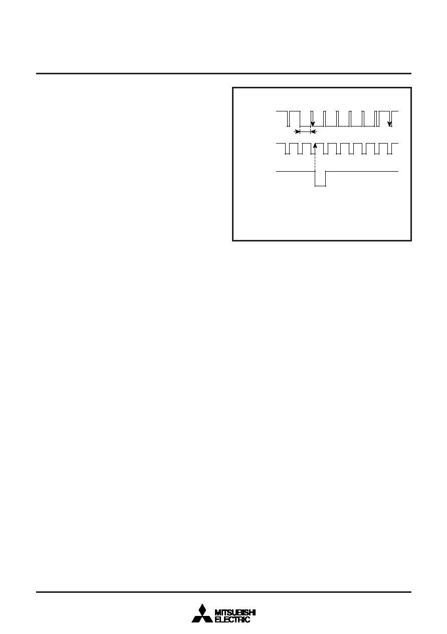
Figure 8.10.6 shows a Vsep generating timing. The timing signal shown
in the figure is generated from the reference clock which the timing
generating circuit outputs.
Reading bit 5 of data slicer control register 2 permits determinating
the shape of the V-pulse portion of the composite sync signal. As
shown in Figure 8.10.7, when the A level matches the B level, this bit
is “0.” In the case of a mismatch, the bit is “1.”
Fig. 8.10.6 Vsep Generating Timing (method 2)
Composite s
Timing
signal
Vsep signal
Measure LOW period
A Vsep signal is generated at a rising of the timing signal
immediately after the LOW level width of the composite
sync signal exceeds a certain time.
相關(guān)PDF資料 |
PDF描述 |
|---|---|
| MB90F428GBPFV | 16-BIT, FLASH, 16 MHz, MICROCONTROLLER, PQFP100 |
| MB90F423GBPFV | 16-BIT, FLASH, 16 MHz, MICROCONTROLLER, PQFP100 |
| MB90423GBPFV | 16-BIT, MROM, 16 MHz, MICROCONTROLLER, PQFP100 |
| MB90427GBPFV | 16-BIT, MROM, 16 MHz, MICROCONTROLLER, PQFP100 |
| MB90F423GBPF | 16-BIT, FLASH, 16 MHz, MICROCONTROLLER, PQFP100 |
相關(guān)代理商/技術(shù)參數(shù) |
參數(shù)描述 |
|---|---|
| MB90F428GAPMC-GSE1 | 制造商:FUJITSU 功能描述: |
| MB90F428GCPFR-GSE1 | 制造商:FUJITSU 功能描述: |
| MB90F438LSPFR-GE1 | 制造商:FUJITSU 功能描述: |
| MB90F438LSPMCR-GE1 | 制造商:FUJITSU 功能描述: |
| MB90F439PMCR-GE1 | 制造商:FUJITSU 功能描述: |
發(fā)布緊急采購(gòu),3分鐘左右您將得到回復(fù)。