- 您現(xiàn)在的位置:買(mǎi)賣(mài)IC網(wǎng) > PDF目錄369889 > M68HC001 (Motorola, Inc.) 16-/32-Bit Microprocessor(16/32位微處理器) PDF資料下載
參數(shù)資料
| 型號(hào): | M68HC001 |
| 廠商: | Motorola, Inc. |
| 英文描述: | 16-/32-Bit Microprocessor(16/32位微處理器) |
| 中文描述: | 16/32位微處理器(16/32位微處理器) |
| 文件頁(yè)數(shù): | 165/184頁(yè) |
| 文件大?。?/td> | 1006K |
| 代理商: | M68HC001 |
第1頁(yè)第2頁(yè)第3頁(yè)第4頁(yè)第5頁(yè)第6頁(yè)第7頁(yè)第8頁(yè)第9頁(yè)第10頁(yè)第11頁(yè)第12頁(yè)第13頁(yè)第14頁(yè)第15頁(yè)第16頁(yè)第17頁(yè)第18頁(yè)第19頁(yè)第20頁(yè)第21頁(yè)第22頁(yè)第23頁(yè)第24頁(yè)第25頁(yè)第26頁(yè)第27頁(yè)第28頁(yè)第29頁(yè)第30頁(yè)第31頁(yè)第32頁(yè)第33頁(yè)第34頁(yè)第35頁(yè)第36頁(yè)第37頁(yè)第38頁(yè)第39頁(yè)第40頁(yè)第41頁(yè)第42頁(yè)第43頁(yè)第44頁(yè)第45頁(yè)第46頁(yè)第47頁(yè)第48頁(yè)第49頁(yè)第50頁(yè)第51頁(yè)第52頁(yè)第53頁(yè)第54頁(yè)第55頁(yè)第56頁(yè)第57頁(yè)第58頁(yè)第59頁(yè)第60頁(yè)第61頁(yè)第62頁(yè)第63頁(yè)第64頁(yè)第65頁(yè)第66頁(yè)第67頁(yè)第68頁(yè)第69頁(yè)第70頁(yè)第71頁(yè)第72頁(yè)第73頁(yè)第74頁(yè)第75頁(yè)第76頁(yè)第77頁(yè)第78頁(yè)第79頁(yè)第80頁(yè)第81頁(yè)第82頁(yè)第83頁(yè)第84頁(yè)第85頁(yè)第86頁(yè)第87頁(yè)第88頁(yè)第89頁(yè)第90頁(yè)第91頁(yè)第92頁(yè)第93頁(yè)第94頁(yè)第95頁(yè)第96頁(yè)第97頁(yè)第98頁(yè)第99頁(yè)第100頁(yè)第101頁(yè)第102頁(yè)第103頁(yè)第104頁(yè)第105頁(yè)第106頁(yè)第107頁(yè)第108頁(yè)第109頁(yè)第110頁(yè)第111頁(yè)第112頁(yè)第113頁(yè)第114頁(yè)第115頁(yè)第116頁(yè)第117頁(yè)第118頁(yè)第119頁(yè)第120頁(yè)第121頁(yè)第122頁(yè)第123頁(yè)第124頁(yè)第125頁(yè)第126頁(yè)第127頁(yè)第128頁(yè)第129頁(yè)第130頁(yè)第131頁(yè)第132頁(yè)第133頁(yè)第134頁(yè)第135頁(yè)第136頁(yè)第137頁(yè)第138頁(yè)第139頁(yè)第140頁(yè)第141頁(yè)第142頁(yè)第143頁(yè)第144頁(yè)第145頁(yè)第146頁(yè)第147頁(yè)第148頁(yè)第149頁(yè)第150頁(yè)第151頁(yè)第152頁(yè)第153頁(yè)第154頁(yè)第155頁(yè)第156頁(yè)第157頁(yè)第158頁(yè)第159頁(yè)第160頁(yè)第161頁(yè)第162頁(yè)第163頁(yè)第164頁(yè)當(dāng)前第165頁(yè)第166頁(yè)第167頁(yè)第168頁(yè)第169頁(yè)第170頁(yè)第171頁(yè)第172頁(yè)第173頁(yè)第174頁(yè)第175頁(yè)第176頁(yè)第177頁(yè)第178頁(yè)第179頁(yè)第180頁(yè)第181頁(yè)第182頁(yè)第183頁(yè)第184頁(yè)
MOTOROLA
M68000 8-/16-/32-BIT MICROPROCESSORS USER'S MANUAL
10-25
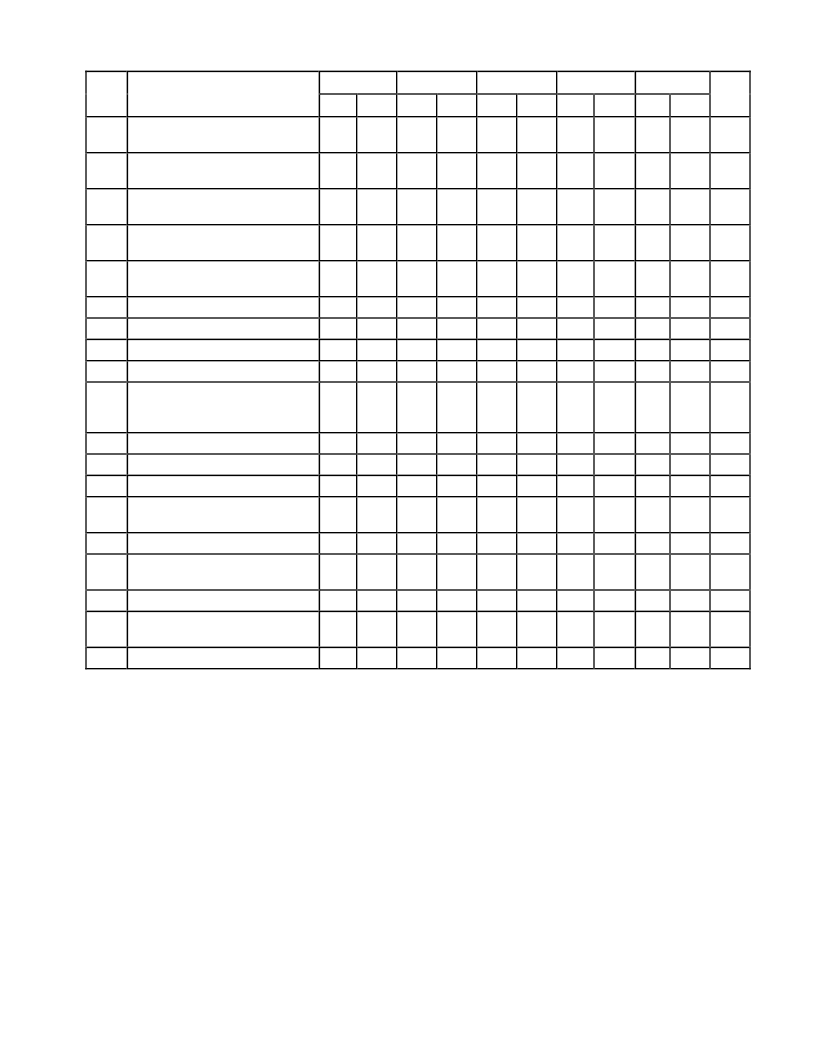
Num
Characteristic
8 MHz
10 MHz
12.5 MHz
16.67 MHz
20 MHz
Unit
Min
Max
Min
Max
Min
Max
Min
Max
Min
Max
29
AS, DS
Negated to Data-In Invalid
(Hold Time on Read)
0
—
0
—
0
—
0
—
0
—
ns
29A
AS, DS
Negated to Data-In High
Impedance
—
187
—
150
—
120
—
90
—
75
ns
30
AS, DS
Negated to
BERR
Negated
0
—
0
—
0
—
0
—
0
—
ns
312,5
DTACK
Asserted to Data-In Valid
(Setup Time)
—
90
—
65
—
50
—
50
—
42
ns
32
HALT
and
RESET
Input Transition
Time
0
150
0
150
0
150
0
150
0
150
ns
33
Clock High to
BG
Asserted
—
35
—
35
—
35
0
30
0
25
ns
34
Clock High to
BG
Negated
—
35
—
35
—
35
0
30
0
25
ns
35
367
BR
Asserted to
BG
Asserted
1.5
3.5
1.5
3.5
1.5
3.5
1.5
3.5
1.5
3.5
Clks
BR
Negated to
BG
Negated
1.5
3.5
1.5
3.5
1.5
3.5
1.5
3.5
1.5
3.5
Clks
38
BG
Asserted to Control, Address,
Data Bus High Impedance (
AS
Negated)
—
55
—
55
—
55
—
50
—
42
ns
39
BG
Width Negated
1.5
1.5
1.5
1.5
1.5
—
Clks
44
475
482,3
AS, DS
Negated to
VPA
Negated
0
55
0
55
0
55
0
50
0
42
ns
Asynchronous Input Setup Time
5
—
5
—
5
—
5
—
5
—
ns
BERR
Asserted to
DTACK
Asserted
20
—
20
—
20
—
10
—
10
—
ns
53
Data-Out Hold from Clock High
0
—
0
—
0
—
0
—
0
—
ns
55
R/
W
Asserted to Data Bus
Impedance Change
30
—
20
—
10
—
0
—
0
—
ns
564
587
HALT/RESET
Pulse Width
10
—
10
—
10
—
10
—
10
—
Clks
BR
Negated to
AS, DS
, R/
W
Driven
1.5
—
1.5
—
1.5
—
1.5
—
1.5
—
Clks
58A7
BR
Negated to FC,
VMA
Driven
1
—
1
—
1
—
1
—
1
—
Clks
NOTES:1. For a loading capacitance of less than or equal to 50 pF, subtract 5 ns from the value given in the
maximum columns.
2. Actual value depends on clock period.
3.I f #47 is satisfied for both
DTACK
and
BERR
, #48 may be ignored. In the absence of
DTACK, BERR
is an
asynchronous input using the asynchronous input setup time (#47).
4. For power-up, the MC68EC000 must be held in the reset state for 520 clocks to allow stabilization of on-
chip circuitry. After the system is powered up, #56 refers to the minimum pulse width required to
reset the processor.
5. If the asynchronous input setup time (#47) requirement is satisfied for
DTACK
, the
DTACK
-asserted to data
setup time (#31) requirement can be ignored. The data must only satisfy the data-in to clock low
setup time (#27) for the following clock cycle.
6. When
AS
and R/
W
are equally loaded (
±
20;pc), subtract 5 ns from the values given in these columns.
7. The minimum value must be met to guarantee proper operation. If the maximum value is exceeded,
BG
may be reasserted.
8.
DS
is used in this specification to indicate
UDS
and
LDS
.
相關(guān)PDF資料 |
PDF描述 |
|---|---|
| M68EC000 | 16/32 Bit Microprocesso(16/32位微處理器) |
| M68HC16 | 16-Bit Microcontroller(16位微控制器) |
| MAC08BT1 | TRIAC 0.8 AMPERE RMS 200 thru 600 Volts |
| MAC08MT1 | SENSITIVE GATE TRIACS |
| MAC08DT1 | TRIAC 0.8 AMPERE RMS 200 thru 600 Volts |
相關(guān)代理商/技術(shù)參數(shù) |
參數(shù)描述 |
|---|---|
| M68HC05 | 制造商:FREESCALE 制造商全稱(chēng):Freescale Semiconductor, Inc 功能描述:Microcontrollers |
| M68HC05_13 | 制造商:FREESCALE 制造商全稱(chēng):Freescale Semiconductor, Inc 功能描述:M68HC05 Microcontrollers |
| M68HC05EVS | 制造商:MOTOROLA 制造商全稱(chēng):Motorola, Inc 功能描述:Motorola M68HC05 Family Evaluation System |
| M68HC05M68H | 制造商:MOTOROLA 制造商全稱(chēng):Motorola, Inc 功能描述:HCMOS Microcontroller Unit |
| M68HC08 | 制造商:FREESCALE 制造商全稱(chēng):Freescale Semiconductor, Inc 功能描述:Microcontrollers |
發(fā)布緊急采購(gòu),3分鐘左右您將得到回復(fù)。