- 您現在的位置:買賣IC網 > PDF目錄45043 > M38198ECFS 8-BIT, UVPROM, 4.2 MHz, MICROCONTROLLER, CQCC100 PDF資料下載
參數資料
| 型號: | M38198ECFS |
| 元件分類: | 微控制器/微處理器 |
| 英文描述: | 8-BIT, UVPROM, 4.2 MHz, MICROCONTROLLER, CQCC100 |
| 封裝: | CERAMIC, LCC-100 |
| 文件頁數: | 80/218頁 |
| 文件大小: | 2137K |
| 代理商: | M38198ECFS |
第1頁第2頁第3頁第4頁第5頁第6頁第7頁第8頁第9頁第10頁第11頁第12頁第13頁第14頁第15頁第16頁第17頁第18頁第19頁第20頁第21頁第22頁第23頁第24頁第25頁第26頁第27頁第28頁第29頁第30頁第31頁第32頁第33頁第34頁第35頁第36頁第37頁第38頁第39頁第40頁第41頁第42頁第43頁第44頁第45頁第46頁第47頁第48頁第49頁第50頁第51頁第52頁第53頁第54頁第55頁第56頁第57頁第58頁第59頁第60頁第61頁第62頁第63頁第64頁第65頁第66頁第67頁第68頁第69頁第70頁第71頁第72頁第73頁第74頁第75頁第76頁第77頁第78頁第79頁當前第80頁第81頁第82頁第83頁第84頁第85頁第86頁第87頁第88頁第89頁第90頁第91頁第92頁第93頁第94頁第95頁第96頁第97頁第98頁第99頁第100頁第101頁第102頁第103頁第104頁第105頁第106頁第107頁第108頁第109頁第110頁第111頁第112頁第113頁第114頁第115頁第116頁第117頁第118頁第119頁第120頁第121頁第122頁第123頁第124頁第125頁第126頁第127頁第128頁第129頁第130頁第131頁第132頁第133頁第134頁第135頁第136頁第137頁第138頁第139頁第140頁第141頁第142頁第143頁第144頁第145頁第146頁第147頁第148頁第149頁第150頁第151頁第152頁第153頁第154頁第155頁第156頁第157頁第158頁第159頁第160頁第161頁第162頁第163頁第164頁第165頁第166頁第167頁第168頁第169頁第170頁第171頁第172頁第173頁第174頁第175頁第176頁第177頁第178頁第179頁第180頁第181頁第182頁第183頁第184頁第185頁第186頁第187頁第188頁第189頁第190頁第191頁第192頁第193頁第194頁第195頁第196頁第197頁第198頁第199頁第200頁第201頁第202頁第203頁第204頁第205頁第206頁第207頁第208頁第209頁第210頁第211頁第212頁第213頁第214頁第215頁第216頁第217頁第218頁
156
2. APPLICATION
MITSUBISHI MICROCOMPUTER
3819 Group
2.9 Clock generating circuit
3819 Group USER’S MANUAL
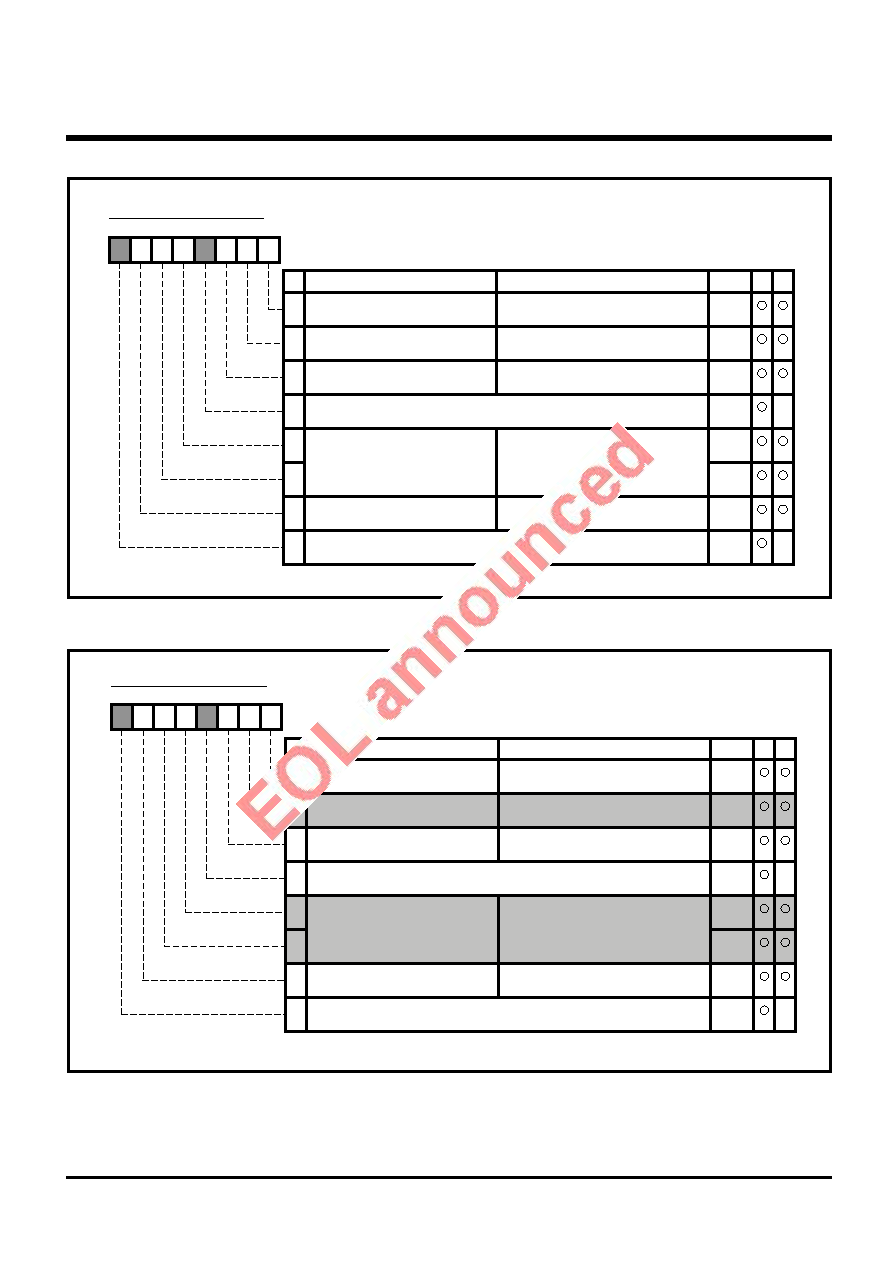
Fig. 2.9.4 Structure of Timer 34 mode register
Fig. 2.9.3 Structure of Timer 12 mode register
Timer 12 mode register
b7 b6 b5 b4 b3 b2 b1 b0
B
Function
At reset
RW
0
1
2
3
4
5
6
7
0
Timer 12 mode register (T12M) [Address:2816
]
Name
Timer 1 count stop bit
Timer 2 count stop bit
Timer 1 count source
selection bit
Timer 2 count source
selection bits
Timer 1 output selection bit
(P46)
0 : Operating
1 : Stopped
0 : Operating
1 : Stopped
0 : f(XIN)/16 or f(XCIN)/16
1 : f(XCIN)
00 : Timer 1 underflow
01 : f(XCIN)
10 : External count input CNTR 0
11 : Not available
0 : I/O port
1 : Timer 1 output
b5 b4
Nothing is allocated for this bit. This is a write disabled bit.
When this bit is read out, the value is "0."
Nothing is allocated for this bit. This is a write disabled bit.
When this bit is read out, the value is "0."
!
Timer 34 mode register
b7 b6 b5 b4 b3 b2 b1 b0
B
Function
At reset
RW
0
1
2
3
4
5
6
7
0
Timer 34 mode register (T34M) [Address:2916
]
Name
Timer 3 count stop bit
Timer 4 count stop bit
Timer 3 count source
selection bit
Timer 4 count source
selection bits
Timer 3 output selection bit
(P47)
0 : Operating
1 : Stopped
0 : Operating
1 : Stopped
0 : f(XIN)/16 or f(XCIN)/16
1 : Timer 2 underflow
00 : f(XIN)/16 or f(XCIN)/16
01 : Timer 3 underflow
10 : External count input CNTR 1
11 : Not available
0 : I/O port
1 : Timer 3 output
b5 b4
Nothing is allocated for this bit. This is a write disabled bit.
When this bit is read out, the value is "0."
Nothing is allocated for this bit. This is a write disabled bit.
When this bit is read out, the value is "0."
!
相關PDF資料 |
PDF描述 |
|---|---|
| M38199MF-XXXFP | 8-BIT, MROM, 4.2 MHz, MICROCONTROLLER, PQFP100 |
| M38199EFFP | 8-BIT, OTPROM, MICROCONTROLLER, PQFP100 |
| M38198EC-XXXFP | 8-BIT, OTPROM, MICROCONTROLLER, PQFP100 |
| M38199MF-XXXKP | 8-BIT, MROM, MICROCONTROLLER, PQFP100 |
| M38198MC-XXXKP | 8-BIT, MROM, MICROCONTROLLER, PQFP100 |
相關代理商/技術參數 |
參數描述 |
|---|---|
| M38198MCA809 | 制造商:Panasonic Industrial Company 功能描述:IC |
| M38198MCA824 | 制造商:Panasonic Industrial Company 功能描述:IC |
| M38198MCA827 | 制造商:Panasonic Industrial Company 功能描述:IC |
| M38199MF072F | 制造商:Panasonic Industrial Company 功能描述:IC |
| M38199MF210F | 制造商:Panasonic Industrial Company 功能描述:IC |
發(fā)布緊急采購,3分鐘左右您將得到回復。