- 您現(xiàn)在的位置:買賣IC網(wǎng) > PDF目錄69014 > M37643M8-XXXHP 8-BIT, MROM, 12 MHz, MICROCONTROLLER, PQFP80 PDF資料下載
參數(shù)資料
| 型號: | M37643M8-XXXHP |
| 元件分類: | 微控制器/微處理器 |
| 英文描述: | 8-BIT, MROM, 12 MHz, MICROCONTROLLER, PQFP80 |
| 封裝: | 12 X 12 MM, 0.50 MM PITCH, PLASTIC, LQFP-80 |
| 文件頁數(shù): | 78/123頁 |
| 文件大?。?/td> | 1292K |
| 代理商: | M37643M8-XXXHP |
第1頁第2頁第3頁第4頁第5頁第6頁第7頁第8頁第9頁第10頁第11頁第12頁第13頁第14頁第15頁第16頁第17頁第18頁第19頁第20頁第21頁第22頁第23頁第24頁第25頁第26頁第27頁第28頁第29頁第30頁第31頁第32頁第33頁第34頁第35頁第36頁第37頁第38頁第39頁第40頁第41頁第42頁第43頁第44頁第45頁第46頁第47頁第48頁第49頁第50頁第51頁第52頁第53頁第54頁第55頁第56頁第57頁第58頁第59頁第60頁第61頁第62頁第63頁第64頁第65頁第66頁第67頁第68頁第69頁第70頁第71頁第72頁第73頁第74頁第75頁第76頁第77頁當(dāng)前第78頁第79頁第80頁第81頁第82頁第83頁第84頁第85頁第86頁第87頁第88頁第89頁第90頁第91頁第92頁第93頁第94頁第95頁第96頁第97頁第98頁第99頁第100頁第101頁第102頁第103頁第104頁第105頁第106頁第107頁第108頁第109頁第110頁第111頁第112頁第113頁第114頁第115頁第116頁第117頁第118頁第119頁第120頁第121頁第122頁第123頁
Rev.2.00
Aug 28, 2006
page 56 of 119
7643 Group
REJ03B0054-0200
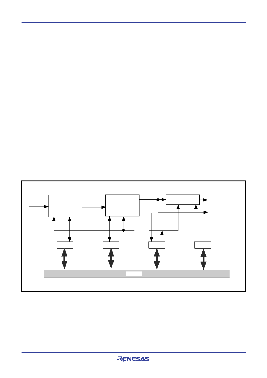
FREQUENCY SYNTHESIZER (PLL)
The frequency synthesizer generates the 48 MHz clock required
by fUSB and fSYN, which are multiples of the external input refer-
ence f(XIN). Figure 51 shows the block diagram for the frequency
synthesizer circuit.
The Frequency Synthesizer Input Bit selects either f(XIN) or
f(XCIN) as an input clock fIN for the frequency synthesizer.
The Frequency Synthesizer Multiply Register 2 (FSM2: address
006E16) divides fIN to generate fPIN, where
fPIN = fIN / 2(n + 1), n: value set to FSM2.
When the value of Frequency Synthesizer Multiply Register 2 is
set to 255, the division is not performed and fPIN will equal fIN.
fVCO is generated according to the contents of Frequency Synthe-
sizer Multiply Register 1 (FSM1: address 006D16), where
fVCO = fPIN {2(n + 1)}, n: value set to FSM1.
Set the value of FSM1 so that the value of fVCO is 48 MHz.
fSYN is generated according to the contents of the Frequency Syn-
thesizer Divide Register (FSD: address 006F16), where
fSYN = fVCO / 2(m + 1), m: value set to FSD.
When the value of the Frequency Synthesizer Divide Register is
set to 255, the division is not performed and fSYN becomes invalid.
[Frequency Synthesizer Control Register] FSC
Setting the Frequency Synthesizer Enable Bit (FSE) to “1” enables
the frequency synthesizer. When the Frequency Synthesizer Lock
Status Bit (LS) is “1” in the frequency synthesizer enabled, this in-
dicates that fSYN and fVCO have correct frequencies.
sNotes
Make sure to connect a low-pulse filter to the LPF pin when using
the frequency synthesizer. In addition, please refer to “Program-
ming Notes: Frequency Synthesizer” when recovering from a
Hardware Reset.
FSM2
Data Bus
FSM1
FSC
Prescaler
fIN
fPIN
fVCO
fSYN
fUSB
(address 006E16)
(address 006D16)
(address 006C16)
(address 006F16)
FSD
Frequency
Multiplier
Frequency Divider
F
re
q
u
e
n
c
y
s
y
n
th
e
s
iz
e
r
lo
c
k
s
ta
tu
s
b
it
Fig. 51 Frequency synthesizer block diagram
相關(guān)PDF資料 |
PDF描述 |
|---|---|
| M37643F8HP | 8-BIT, FLASH, 12 MHz, MICROCONTROLLER, PQFP80 |
| M37700E2AFS | 16-BIT, UVPROM, 16 MHz, MICROCONTROLLER, CQCC80 |
| M37700E2AXXXFP | 16-BIT, OTPROM, 16 MHz, MICROCONTROLLER, PQFP80 |
| M37701E2-XXXSP | 16-BIT, OTPROM, 8 MHz, MICROCONTROLLER, PDIP64 |
| M37702E4EXXXFP | 16-BIT, OTPROM, 16 MHz, MICROCONTROLLER, PQFP80 |
相關(guān)代理商/技術(shù)參數(shù) |
參數(shù)描述 |
|---|---|
| M3764A-12 | 制造商:OK International 功能描述: |
| M3765 | 制造商:未知廠家 制造商全稱:未知廠家 功能描述:HORN/SIREN WITH SOFT CHIRP 6 ALARM SOUNDS |
| M3766 | 制造商:未知廠家 制造商全稱:未知廠家 功能描述:HORN/SIREN WITH SOFT CHIRP 6 ALARM SOUNDS |
| M37702E2LGP | 制造商:Mitsubishi Electric 功能描述: |
| M37702E4BFS | 制造商:Renesas Electronics Corporation 功能描述:EPROM MCU/8BIT CMOS EMULATION CHIP - Bulk |
發(fā)布緊急采購,3分鐘左右您將得到回復(fù)。