- 您現(xiàn)在的位置:買賣IC網(wǎng) > PDF目錄69010 > M34506E4FP 4-BIT, OTPROM, MICROCONTROLLER, PDSO20 PDF資料下載
參數(shù)資料
| 型號: | M34506E4FP |
| 元件分類: | 微控制器/微處理器 |
| 英文描述: | 4-BIT, OTPROM, MICROCONTROLLER, PDSO20 |
| 封裝: | 5.30 X 12.60 MM, 1.27 MM PITCH, PLASTIC, SOP-20 |
| 文件頁數(shù): | 41/114頁 |
| 文件大小: | 937K |
| 代理商: | M34506E4FP |
第1頁第2頁第3頁第4頁第5頁第6頁第7頁第8頁第9頁第10頁第11頁第12頁第13頁第14頁第15頁第16頁第17頁第18頁第19頁第20頁第21頁第22頁第23頁第24頁第25頁第26頁第27頁第28頁第29頁第30頁第31頁第32頁第33頁第34頁第35頁第36頁第37頁第38頁第39頁第40頁當(dāng)前第41頁第42頁第43頁第44頁第45頁第46頁第47頁第48頁第49頁第50頁第51頁第52頁第53頁第54頁第55頁第56頁第57頁第58頁第59頁第60頁第61頁第62頁第63頁第64頁第65頁第66頁第67頁第68頁第69頁第70頁第71頁第72頁第73頁第74頁第75頁第76頁第77頁第78頁第79頁第80頁第81頁第82頁第83頁第84頁第85頁第86頁第87頁第88頁第89頁第90頁第91頁第92頁第93頁第94頁第95頁第96頁第97頁第98頁第99頁第100頁第101頁第102頁第103頁第104頁第105頁第106頁第107頁第108頁第109頁第110頁第111頁第112頁第113頁第114頁
Rev.2.00
Aug 28, 2006
page 28 of 119
7643 Group
REJ03B0054-0200
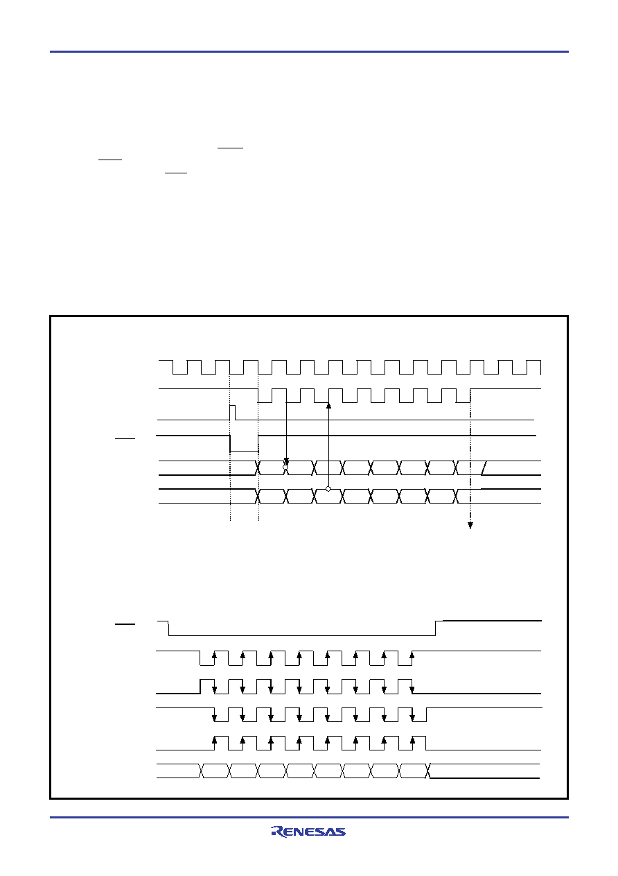
Serial I/O Normal Operation
The serial I/O counter is set to “7” by writing operation to the serial
I/O shift register (address 002A16). When the SRDY Output Select
bit is “1”, the SRDY pin goes “L” after that writing. On the negative
edge of the transfer clock the SRDY pin returns “H” and the data
of the first bit is transmitted from the STXD pin. The remaining
data are done from the STXD pin bit by bit on each falling edge of
the transfer clock.
Additionally, the data is latched from the SRXD pin on each rising
edge of the transfer clock and then the contents of the serial I/O
shift register are shifted by one bit.
When the internal system clock is selected as the transfer clock,
the followings occur at counting eight transfer clocks:
The serial I/O counter reaches “0”
The transfer clock halts at “H”
The serial I/O interrupt request bit is set to “1”
The STXD pin goes a high-impedance state after an 8-bit transfer
is completed.
When the external clock is selected as the transfer clock, the fol-
lowings occur at counting eight transfer clocks:
The serial I/O counter reaches “0”
The serial I/O interrupt request bit is set to “1”
In this case, the transfer clock needs to be controlled by the exter-
nal source because the transfer clock does not halt. Additionally,
the STXD pin does not go a high-impedance state after an 8-bit
transfer is completed.
Figure 23 shows serial I/O timing.
Fig. 23 Serial I/O timing
D1
D0
D2
D3
D4
D5
D6
D7
First
Last
STXD/SRXD
Synchronizing clock
SCLK (CPoL = 1, CPha =1 )
SCLK (CPoL = 0, CPha = 1)
SCLK (CPoL = 1, CPha = 0)
SCLK (CPoL = 0, CPha = 0)
qNormal mode timing (LSB first)
Transfer clock
Synchronizing clock
Serial I/O shift
register write signal
SRDY signal
Serial I/O output STXD
Serial I/O input SRXD
(Note)
Interrupt request bit is set to “1”.
Note: When the internal clock is selected as the transfer clock, the STXD pin goes to a high-impedance state after transfer completion.
qSPI compatible mode timing
SRDY signal
相關(guān)PDF資料 |
PDF描述 |
|---|---|
| M34508G4HFP | 4-BIT, MROM, 6 MHz, MICROCONTROLLER, PDSO20 |
| M34508G4GP | 4-BIT, MROM, 6 MHz, MICROCONTROLLER, PDSO20 |
| M34508G4H-XXXFP | 4-BIT, MROM, 6 MHz, MICROCONTROLLER, PDSO20 |
| M34508G4-XXXFP | 4-BIT, MROM, 6 MHz, MICROCONTROLLER, PDSO20 |
| M34508G4FP | 4-BIT, MROM, 6 MHz, MICROCONTROLLER, PDSO20 |
相關(guān)代理商/技術(shù)參數(shù) |
參數(shù)描述 |
|---|---|
| M34506M2 | 制造商:RENESAS 制造商全稱:Renesas Technology Corp 功能描述:SINGLE-CHIP 4-BIT CMOS MICROCOMPUTER |
| M34506M2-XXXFP | 制造商:RENESAS 制造商全稱:Renesas Technology Corp 功能描述:4-BIT CISC SINGLE-CHIP MICROCOMPUTER 4500 SERIES |
| M34506M4 | 制造商:RENESAS 制造商全稱:Renesas Technology Corp 功能描述:SINGLE-CHIP 4-BIT CMOS MICROCOMPUTER |
| M34506M4-XXXFP | 制造商:RENESAS 制造商全稱:Renesas Technology Corp 功能描述:4-BIT CISC SINGLE-CHIP MICROCOMPUTER 4500 SERIES |
| M34507E4FP | 制造商:RENESAS 制造商全稱:Renesas Technology Corp 功能描述:SINGLE-CHIP 4-BIT CMOS MICROCOMPUTER |
發(fā)布緊急采購,3分鐘左右您將得到回復(fù)。