- 您現(xiàn)在的位置:買賣IC網(wǎng) > PDF目錄369873 > LV8572AVX Real-Time Clock PDF資料下載
參數(shù)資料
| 型號(hào): | LV8572AVX |
| 英文描述: | Real-Time Clock |
| 中文描述: | 實(shí)時(shí)時(shí)鐘 |
| 文件頁(yè)數(shù): | 8/24頁(yè) |
| 文件大小: | 353K |
| 代理商: | LV8572AVX |
第1頁(yè)第2頁(yè)第3頁(yè)第4頁(yè)第5頁(yè)第6頁(yè)第7頁(yè)當(dāng)前第8頁(yè)第9頁(yè)第10頁(yè)第11頁(yè)第12頁(yè)第13頁(yè)第14頁(yè)第15頁(yè)第16頁(yè)第17頁(yè)第18頁(yè)第19頁(yè)第20頁(yè)第21頁(yè)第22頁(yè)第23頁(yè)第24頁(yè)

Functional Description
(Continued)
The oscillator is programmed via the Real Time Mode Reg-
ister to operate at various frequencies. The crystal oscillator
is designed to offer optimum performance at each frequen-
cy. Thus, at 32.768 kHz the oscillator is configured as a low
frequency and low power oscillator. At the higher frequen-
cies the oscillator inverter is reconfigured. In addition to the
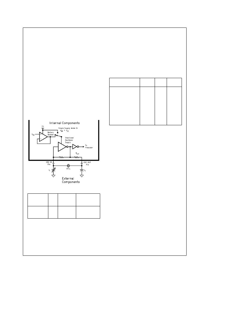
inverter, the oscillator feedback bias resistor is included on
chip, as shown inFigure 4. The oscillator input may be driv-
en from an external source if desired. Refer to test mode
application note for details. The oscillator stability is en-
hanced through the use of an on chip regulated power sup-
ply.
The typical range of trimmer capacitor (as shown in Oscilla-
tor Circuit DiagramFigure 4, and in the typical application) at
the oscillator input pin is suggested only to allow accurate
tuning of the oscillator. This range is based on a typical
printed circuit board layout and may have to be changed
depending on the parasitic capacitance of the printed circuit
board or fixture being used. In all cases, the
load capaci-
tance
specified by the crystal manufacturer (nominal value
11 pF for the 32.768 crystal) is what determines proper os-
cillation. This load capcitance is the series combination of
capacitance on each side of the crystal (with respect to
ground).
TL/F/11416–8
FIGURE 4. Oscillator Circuit Diagram
R
OUT
(Switched
Internally)
XTAL
C
o
C
t
32/32.768 kHz
4.194304 MHz
4.9152 MHz
47 pF
68 pF
68 pF
2 pF–22 pF
0 pF–80 pF
29 pF–49 pF
150 k
X
to 350 k
X
500
X
to 900
X
500
X
to 900
X
INTERRUPT LOGIC FUNCTIONAL DESCRIPTION
The TCP has the ability to coordinate processor timing ac-
tivities. To enhance this, an interrupt structure has been im-
plemented which enables several types of events to cause
interrupts. Interrupts are controlled via two Control Regis-
ters in block 1 and two Status Registers in block 0. (See
Register Description for notes on paging and also Figure 5
and Table I.)
The interrupts are enabled by writing a one to the appropri-
ate bits in Interrupt Control Register 0 and/or 1. Any of the
interrupts can be routed to either the INTR pin or the MFO
pin, depending on how the Interrupt Routing register is pro-
grammed. This, for example, enables the user to dedicate
the MFO as a non-maskable interrupt pin to the CPU for
power failure detection and enable all other interrupts to
appear on the INTR pin. The polarity for the active interrupt
can be programmed in the Output Mode Register for either
active high or low, and open drain or push pull outputs.
TABLE I. Registers that are Applicable
to Interrupt Control
Register Name
Register
Select
Page
Select
Address
Main Status Register
Periodic Flag Register
Interrupt Routing
Register
Interrupt Control
Register 0
Interrupt Control
Register 1
Output Mode
Register
X
0
X
0
00H
03H
0
0
04H
1
0
03H
1
0
04H
1
0
02H
The Interrupt Status Flag D0, in the Main Status Register,
indicates the state of INTR and MFO outputs. It is set when
either output becomes active and is cleared when all TCP
interrupts have been cleared and no further interrupts are
pending (i.e., both INTR and MFO are returned to their inac-
tive state). This flag enables the TCP to be rapidly polled by
the
m
P to determine the source of an interrupt in a wiredD
OR interrupt system.
Note that the Interrupt Status Flag will only monitor the state
of the MFO output if it has been configured as an interrupt
output (see Output Mode Register description). This is true,
regardless of the state of the Interrupt Routing Register.
Thus the Interrupt Status Flag provides a true reflection of
all conditions routed to the external pins.
Status for the interrupts are provided by the Main Status
Register and the Periodic Flag Register. Bits D1–D5 of the
Main Status Register are the main interrupt bits.
These register bits will be set when their associated timing
events occur. Enabled Alarm or Timer interrupts that occur
will set its Main Status Register bit to a one. However, an
external interrupt will only be generated if the appropriate
Alarm or Timer interrupt enable bits are set (see Figure 5 ).
Disabling the periodic bits will mask the Main Status Regis-
ter periodic bit, but not the Periodic Flag Register bits. The
Power Fail Interrupt bit is set when the interrupt is enabled
and a power fail event has occurred, and is not reset until
the power is restored. If all interrupt enable bits are 0 no
interrupt will be asserted. However, status still can be read
from the Main Status Register in a polled fashion (see Fig-
ure 5 ).
To clear a flag in bits D2–D5 of the Main Status Register a 1
must be written back into the bit location that is to be
cleared. For the Periodic Flag Register reading the status
will reset all the periodic flags.
8
相關(guān)PDF資料 |
PDF描述 |
|---|---|
| LV8800C | Optoelectronic |
| LVA12D | Analog IC |
| LVA12S | Analog IC |
| LVA15D | Analog IC |
| LVA15S | Analog IC |
相關(guān)代理商/技術(shù)參數(shù) |
參數(shù)描述 |
|---|---|
| LV8573A | 制造商:NSC 制造商全稱:National Semiconductor 功能描述:LV8573A Low Voltage Real Time Clock (RTC) |
| LV8573AM | 制造商:NSC 制造商全稱:National Semiconductor 功能描述:LV8573A Low Voltage Real Time Clock (RTC) |
| LV8573AN | 制造商:NSC 制造商全稱:National Semiconductor 功能描述:LV8573A Low Voltage Real Time Clock (RTC) |
| LV8573AV | 制造商:NSC 制造商全稱:National Semiconductor 功能描述:LV8573A Low Voltage Real Time Clock (RTC) |
| LV8573M | 制造商:NSC 制造商全稱:National Semiconductor 功能描述:LV8573A Low Voltage Real Time Clock (RTC) |
發(fā)布緊急采購(gòu),3分鐘左右您將得到回復(fù)。