- 您現(xiàn)在的位置:買賣IC網(wǎng) > PDF目錄369873 > LV8572AVX Real-Time Clock PDF資料下載
參數(shù)資料
| 型號: | LV8572AVX |
| 英文描述: | Real-Time Clock |
| 中文描述: | 實(shí)時時鐘 |
| 文件頁數(shù): | 11/24頁 |
| 文件大小: | 353K |
| 代理商: | LV8572AVX |

Functional Description
(Continued)
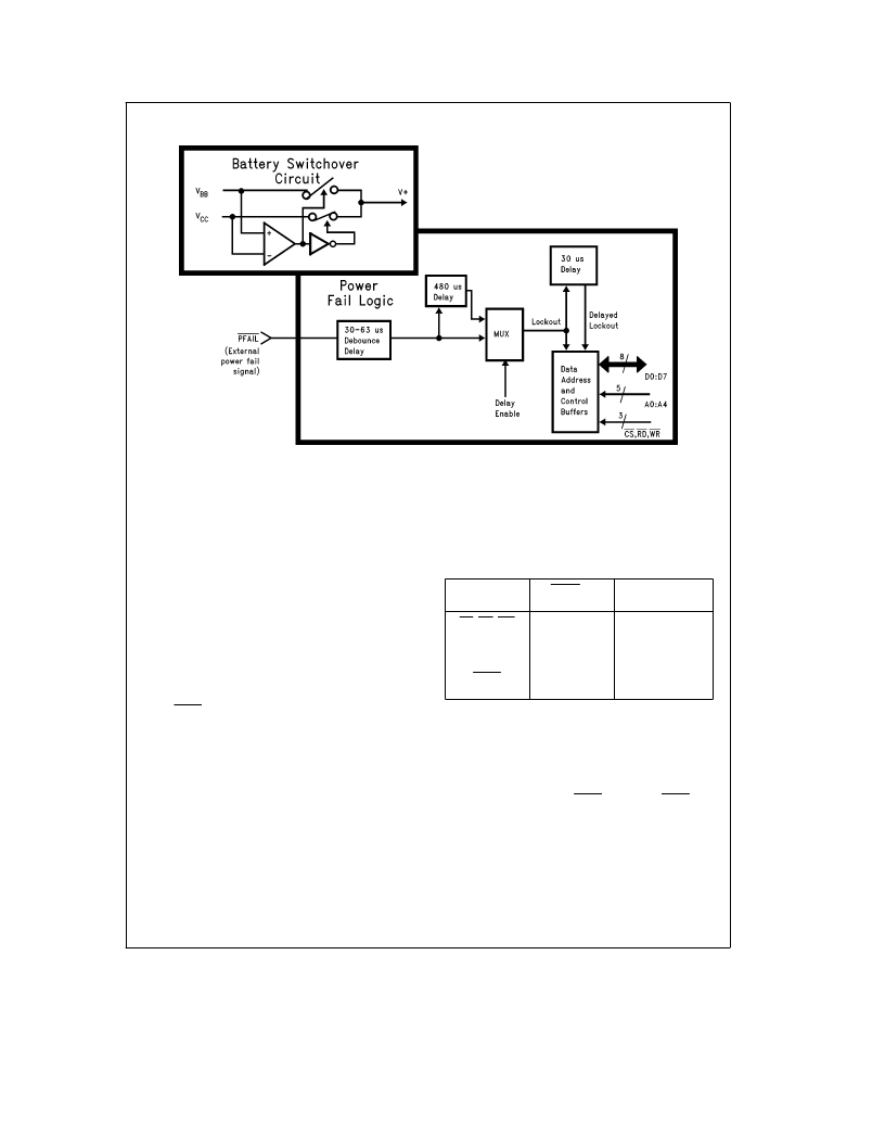
TL/F/11416–10
FIGURE 6. System-Battery Switchover (Upper Left), Power Fail
and Lock-Out Circuits (Lower Right)
The user may choose to have this power failed signal lock-
out the TCP’s data bus within 30
m
s min/63
m
s max or to
delay the lock-out to enable
m
P access after power failure is
detected. This delay is enabled by setting the delay enable
bit in the Routing Register. Also, if the lock-out delay was
not enabled the TCP will disconnect itself from the bus with-
in 30
m
s min
63
m
s max. If chip select is low when a
power failure is detected, a safety circuit will ensure that if a
read or write is held active continuously for greater than
30
m
s after the power fail signal is asserted, the lock-out will
be forced. If a lock-out delay is enabled, the LV8571A will
remain active for 480
m
s after power fail is detected. This
will enable the
m
P to perform last minute bookkeeping be-
fore total system collapse. When the host CPU is finished
accessing the TCP it may force the bus lock-out before
480
m
s has elapsed by resetting the delay enable bit.
The battery switch over circuitry is completely independent
of the PFAIL pin. A separate circuit compares V
CC
to the
V
BB
voltage. As the main supply fails, the TCP will continue
to operate from the V
CC
pin until V
CC
falls below the V
BB
voltage. At this time, the battery supply is switched in, V
CC
is
disconnected, and the device is now in the standby mode. If
indeterminate operation of the battery switch over circuit is
to be avoided, then the voltage at the V
CC
pin must not be
allowed to equal the voltage at the V
BB
pin.
After the generation of a lock-out signal, and eventual
switch in of the battery supply, the pins of the TCP will be
configured as shown in Table II. Outputs that have a pull-up
resistor should be connected to a voltage no greater than
V
BB
.
TABLE II. Pin Isolation during a Power Failure
Pin
PFAIL
e
Logic 0
Standby Mode
V
BB
l
V
CC
CS, RD, WR
A0–A4
D0–D7
Oscillator
PFAIL
INTR, MFO
Locked Out
Locked Out
Locked Out
Not Isolated
Not Isolated
Not Isolated
Locked Out
Locked Out
Locked Out
Not Isolated
Not Isolated
Open Drain
The Timer and Interrupt Power Fail Operation bits in the
Real-Time Mode Register determine whether or not the tim-
ers and interrupts will continue to function after a power fail
event.
As power returns to the system, the battery switch over cir-
cuit will switch back to V
CC
power as soon as it becomes
greater than the battery voltage. The chip will remain in the
locked out state as long as PFAIL
e
0. When PFAIL
e
1
11
相關(guān)PDF資料 |
PDF描述 |
|---|---|
| LV8800C | Optoelectronic |
| LVA12D | Analog IC |
| LVA12S | Analog IC |
| LVA15D | Analog IC |
| LVA15S | Analog IC |
相關(guān)代理商/技術(shù)參數(shù) |
參數(shù)描述 |
|---|---|
| LV8573A | 制造商:NSC 制造商全稱:National Semiconductor 功能描述:LV8573A Low Voltage Real Time Clock (RTC) |
| LV8573AM | 制造商:NSC 制造商全稱:National Semiconductor 功能描述:LV8573A Low Voltage Real Time Clock (RTC) |
| LV8573AN | 制造商:NSC 制造商全稱:National Semiconductor 功能描述:LV8573A Low Voltage Real Time Clock (RTC) |
| LV8573AV | 制造商:NSC 制造商全稱:National Semiconductor 功能描述:LV8573A Low Voltage Real Time Clock (RTC) |
| LV8573M | 制造商:NSC 制造商全稱:National Semiconductor 功能描述:LV8573A Low Voltage Real Time Clock (RTC) |
發(fā)布緊急采購,3分鐘左右您將得到回復(fù)。