- 您現(xiàn)在的位置:買(mǎi)賣IC網(wǎng) > PDF目錄369873 > LV8572AVX Real-Time Clock PDF資料下載
參數(shù)資料
| 型號(hào): | LV8572AVX |
| 英文描述: | Real-Time Clock |
| 中文描述: | 實(shí)時(shí)時(shí)鐘 |
| 文件頁(yè)數(shù): | 18/24頁(yè) |
| 文件大小: | 353K |
| 代理商: | LV8572AVX |
第1頁(yè)第2頁(yè)第3頁(yè)第4頁(yè)第5頁(yè)第6頁(yè)第7頁(yè)第8頁(yè)第9頁(yè)第10頁(yè)第11頁(yè)第12頁(yè)第13頁(yè)第14頁(yè)第15頁(yè)第16頁(yè)第17頁(yè)當(dāng)前第18頁(yè)第19頁(yè)第20頁(yè)第21頁(yè)第22頁(yè)第23頁(yè)第24頁(yè)

Functional Description
(Continued)
D5:
The Delay Enable bit is used when a power fail occurs.
If this bit is set, a 480
m
s delay is generated internally before
the
m
P interface is locked out. This will enable the
m
P to
access the registers for up to 480
m
s after it receives a
power fail interrupt. After a power failure is detected but
prior to the 480
m
s delay timing out, the host
m
P may force
immediate lock out by resetting the Delay Enable bit. Note if
this bit is a 0 when power fails then after a delay of 30
m
s
min/63
m
s max the
m
P cannot read the chip.
D6:
This read only bit is set and reset by the voltage at the
V
BB
pin. It can be used by the
m
P to determine whether the
battery voltage at the V
BB
pin is getting too low. A compara-
tor monitors the battery and when the voltage is lower than
2.1V (typical) this bit is set. The power fail interrupt must be
enabled to check for a low battery voltage.
D7:
Time Save Enable bit controls the loading of real-time-
clock data into the Time Save RAM. When a one is written
to this bit the Time Save RAM will follow the corresponding
clock registers, and when a zero is written to this bit the time
in the Time Save RAM is frozen. This eliminates any syn-
chronization problems when reading the clock, thus negat-
ing the need to check for a counter rollover during a read
cycle.
This bit must be set to a one prior to power failing to enable
the Time Save feature. When the power fails this bit is auto-
matically reset and the time is saved in the Time Save RAM.
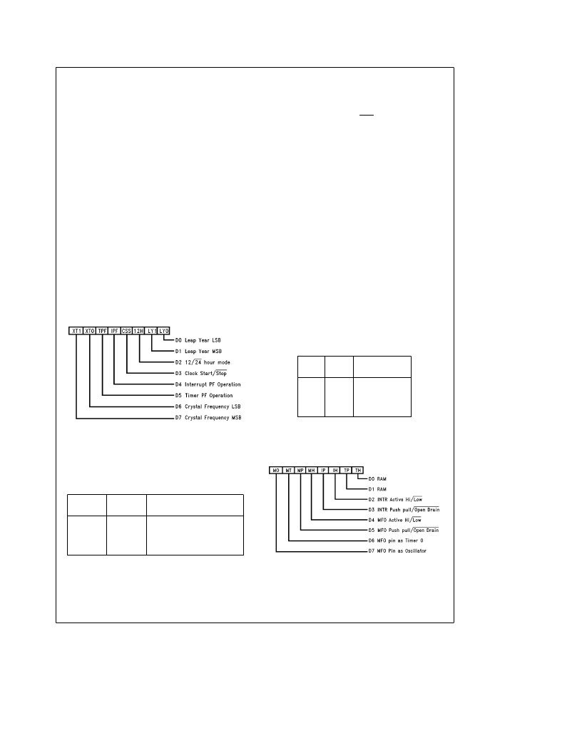
REAL TIME MODE REGISTER
TL/F/11416–20
D0–D1:
These are the leap year counter bits. These bits are
written to set the number of years from the previous leap
year. The leap year counter increments on December 31st
and it internally enables the February 29th counter state.
This method of setting the leap year allows leap year to
occur whenever the user wishes to, thus providing flexibility
in implementing Japanese leap year function.
LY1
LY0
Leap Year
Counter
0
0
1
1
0
1
0
1
Leap Year Current Year
Leap Year Last Year
Leap Year 2 Years Ago
Leap Year 3 Years Ago
D2:
The count mode for the hours counter can be set to
either 24 hour mode or 12 hour mode with AM/PM indicator.
A one will place the clock in 12 hour mode.
D3:
This bit is the master Start/Stop bit for the clock. When
a one is written to this bit the real time counter’s prescaler
and counter chain are enabled. When this bit is reset to zero
the contents of the real time counter is stopped and the
prescaler is cleared. When the TCP is initially powered up
this bit will be held at a logic 0 until the oscillator starts
functioning correctly after which this bit may be modified. If
an oscillator fail event occurs, this bit will be reset to logic 0.
D4:
This bit controls the operation of the interrupt output in
standby mode. If set to a one it allows Alarm, Periodic, and
Power Fail interrupts to be functional in standby mode. Tim-
er interrupts will also be functional provided that bit D5 is
also set. Note that the MFO and INTR pins are configured
as open drain in standby mode.
If bit D4 is set to a zero then interrupt control register 0 and
bits D6 and D7 of interrupt control register 1 will be reset
when the TCP enters the standby mode (V
BB
l
V
CC
). They
will have to be re-configured when system (V
CC
) power is
restored.
D5:
This bit controls the operation of the timers in standby
mode. If set to a one the timers will continue to function
when the TCP is in standby mode. The input pins TCK, G0,
G1 are locked out in standby mode, and cannot be used.
Therefore external control of the timers is not possible in
standby mode. Note also that MFO and T1 pins are auto-
matically reconfigured open drain during standby.
D6 and D7:
These two bits select the crystal clock frequen-
cy as per the following table:
XT1
XT0
Crystal
Frequency
0
0
1
1
0
1
0
1
32.768 kHz
4.194304 MHz
4.9152 MHz
32.000 kHz
All bits are Read/Write, and any mode written into this regis-
ter can be determined by reading the register. On initial
power up these bits are random.
OUTPUT MODE REGISTER
TL/F/11416–21
18
相關(guān)PDF資料 |
PDF描述 |
|---|---|
| LV8800C | Optoelectronic |
| LVA12D | Analog IC |
| LVA12S | Analog IC |
| LVA15D | Analog IC |
| LVA15S | Analog IC |
相關(guān)代理商/技術(shù)參數(shù) |
參數(shù)描述 |
|---|---|
| LV8573A | 制造商:NSC 制造商全稱:National Semiconductor 功能描述:LV8573A Low Voltage Real Time Clock (RTC) |
| LV8573AM | 制造商:NSC 制造商全稱:National Semiconductor 功能描述:LV8573A Low Voltage Real Time Clock (RTC) |
| LV8573AN | 制造商:NSC 制造商全稱:National Semiconductor 功能描述:LV8573A Low Voltage Real Time Clock (RTC) |
| LV8573AV | 制造商:NSC 制造商全稱:National Semiconductor 功能描述:LV8573A Low Voltage Real Time Clock (RTC) |
| LV8573M | 制造商:NSC 制造商全稱:National Semiconductor 功能描述:LV8573A Low Voltage Real Time Clock (RTC) |
發(fā)布緊急采購(gòu),3分鐘左右您將得到回復(fù)。