- 您現(xiàn)在的位置:買賣IC網(wǎng) > PDF目錄383237 > L6566BTR (意法半導(dǎo)體) Multi-mode controller for SMPS PDF資料下載
參數(shù)資料
| 型號(hào): | L6566BTR |
| 廠商: | 意法半導(dǎo)體 |
| 英文描述: | Multi-mode controller for SMPS |
| 中文描述: | 多模式開關(guān)電源控制器 |
| 文件頁數(shù): | 31/51頁 |
| 文件大小: | 401K |
| 代理商: | L6566BTR |
第1頁第2頁第3頁第4頁第5頁第6頁第7頁第8頁第9頁第10頁第11頁第12頁第13頁第14頁第15頁第16頁第17頁第18頁第19頁第20頁第21頁第22頁第23頁第24頁第25頁第26頁第27頁第28頁第29頁第30頁當(dāng)前第31頁第32頁第33頁第34頁第35頁第36頁第37頁第38頁第39頁第40頁第41頁第42頁第43頁第44頁第45頁第46頁第47頁第48頁第49頁第50頁第51頁
L6566B
Application information
31/51
between the detected event and the oscillator, occasionally the device could stop after the
third detection.
This condition is latched as long as the device is supplied. While it is disabled, however, no
energy is coming from the self-supply circuit; hence the voltage on the Vcc capacitor will
decay and cross the UVLO threshold after some time, which clears the latch. The internal
start-up generator is still off, then the Vcc voltage still needs to go below its restart voltage
before the Vcc capacitor is charged again and the device restarted. Ultimately, this will result
in a low-frequency intermittent operation (Hiccup-mode operation), with very low stress on
the power circuit. This special condition is illustrated in the timing diagram of
Figure 18 on
page 30
.
5.8
Frequency modulation
To alleviate converter’s EMI emissions and reduce cost and size of the line filter, it is
advantageous to modulate its switching frequency, so that the resulting spread-spectrum
action distributes the energy of each harmonic of the switching frequency over a number of
side-band harmonics. Their overall energy will be unchanged but the individual amplitudes
will be smaller. This is what naturally occurs with QR operation, due to the twice-mains-
frequency ripple appearing on the input bulk capacitor, which translates into different DCM-
CCM boundary frequencies.
The L6566B is provided with a dedicated pin, FMOD (6), to perform this function if FF mode
is selected.
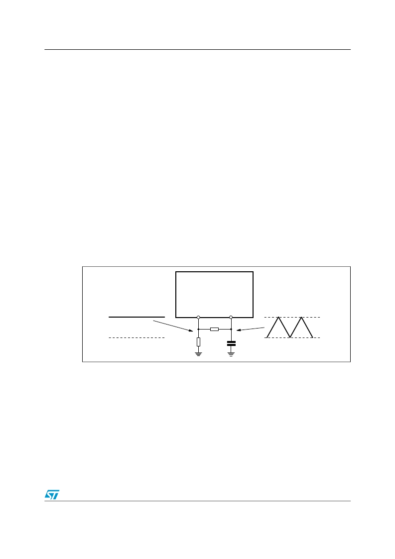
Figure 19. Frequency modulation circuit
With reference to
Figure 19
, the capacitor C
MOD
is connected from FMOD to ground and is
alternately charged and discharged between 0.5 and 1.5 V by internal current generators
sourcing and sinking the same current (three times the current defined by the resistor R
T
on
pin OSC). Hence, the voltage across C
MOD
will be a symmetric triangle, whose frequency f
m
is determined by C
MOD
. By connecting a resistor R
MOD
from FMOD to OSC, the current
sourced by pin OSC will be modulated according a triangular profile at a frequency f
m
. If
R
MOD
is considerably higher than R
T
, as normally is, both f
m
and the symmetry of the
triangle will be little affected.
With this arrangement it is possible to set, nearly independently, the frequency deviation
f
sw
and the modulating frequency f
m
, which define the modulation index:
L6566B
OSC
6
R
T
FMOD
13
R
MOD
C
MOD
1.5 V
0.5 V
0 V
1 V
相關(guān)PDF資料 |
PDF描述 |
|---|---|
| L6567 | HIGH VOLTAGE DRIVER FOR CFL |
| L6567D | HIGH VOLTAGE DRIVER FOR CFL |
| L6571B | High Voltage Half Bridge Driver with Oscillator(帶晶振的高電壓半橋驅(qū)動(dòng)器) |
| L6585D | PFC and Ballast Control IC |
| L6585DTR | PFC and Ballast Control IC |
相關(guān)代理商/技術(shù)參數(shù) |
參數(shù)描述 |
|---|---|
| L6566BTR-CUT TAPE | 制造商:ST 功能描述:L6566B Series 23 V 4.6 mA SMPS Multi-Mode Controller Surface Mount - SOIC-16N |
| L6567 | 制造商:STMICROELECTRONICS 制造商全稱:STMicroelectronics 功能描述:HIGH VOLTAGE DRIVER FOR CFL |
| L6567D | 制造商:STMicroelectronics 功能描述:CFL DRVR 18V 14SOP - Rail/Tube |
| L6569 | 功能描述:功率驅(qū)動(dòng)器IC Hi-Volt Half Bridge RoHS:否 制造商:Micrel 產(chǎn)品:MOSFET Gate Drivers 類型:Low Cost High or Low Side MOSFET Driver 上升時(shí)間: 下降時(shí)間: 電源電壓-最大:30 V 電源電壓-最小:2.75 V 電源電流: 最大功率耗散: 最大工作溫度:+ 85 C 安裝風(fēng)格:SMD/SMT 封裝 / 箱體:SOIC-8 封裝:Tube |
| L6569 | 制造商:STMicroelectronics 功能描述:IC HALF BRIDGE+OSC 6569 DIP8 |
發(fā)布緊急采購(gòu),3分鐘左右您將得到回復(fù)。