- 您現(xiàn)在的位置:買賣IC網(wǎng) > PDF目錄383237 > L6566BTR (意法半導(dǎo)體) Multi-mode controller for SMPS PDF資料下載
參數(shù)資料
| 型號: | L6566BTR |
| 廠商: | 意法半導(dǎo)體 |
| 英文描述: | Multi-mode controller for SMPS |
| 中文描述: | 多模式開關(guān)電源控制器 |
| 文件頁數(shù): | 19/51頁 |
| 文件大?。?/td> | 401K |
| 代理商: | L6566BTR |
第1頁第2頁第3頁第4頁第5頁第6頁第7頁第8頁第9頁第10頁第11頁第12頁第13頁第14頁第15頁第16頁第17頁第18頁當(dāng)前第19頁第20頁第21頁第22頁第23頁第24頁第25頁第26頁第27頁第28頁第29頁第30頁第31頁第32頁第33頁第34頁第35頁第36頁第37頁第38頁第39頁第40頁第41頁第42頁第43頁第44頁第45頁第46頁第47頁第48頁第49頁第50頁第51頁
L6566B
Application information
19/51
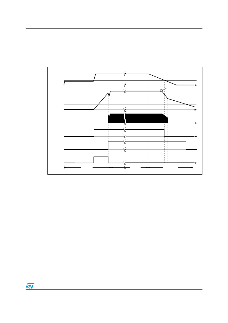
With reference to the timing diagram of
Figure 6
, when power is first applied to the converter
the voltage on the bulk capacitor (Vin) builds up and, at about 80V, the HV generator is
enabled to operate (HV_EN is pulled high) so that it draws about 1 mA. This current, minus
the device’s consumption, charges the bypass capacitor connected from pin Vcc (5) to
ground and makes its voltage rise almost linearly.
Figure 6.
Timing diagram: normal power-up and power-down sequences
As the Vcc voltage reaches the turn-on threshold (14V typ.) the device starts operating and
the HV generator is cut off by the Vcc_OK signal asserted high. The device is powered by
the energy stored in the Vcc capacitor until the self-supply circuit (typically an auxiliary
winding of the transformer and a steering diode) develops a voltage high enough to sustain
the operation. The residual consumption of this circuit is just the one on the 15 M
resistor
(
≈
10 mW at 400 Vdc), typically 50-70 times lower, under the same conditions, as compared
to a standard start-up circuit made with external dropping resistors.
At converter power-down the system will lose regulation as soon as the input voltage is so
low that either peak current or maximum duty cycle limitation is tripped. Vcc will then drop
and stop IC activity as it falls below the UVLO threshold (10V typ.). The Vcc_OK signal is
de-asserted as the Vcc voltage goes below a threshold VCC
rest
located at about 5V. The HV
generator can now restart. However, if Vin < Vin
start
, as illustrated in
Figure 6
, HV_EN is de-
asserted too and the HV generator is disabled. This prevents converter’s restart attempts
and ensures monotonic output voltage decay at power-down in systems where brownout
protection (see the relevant section) is not used.
The low restart threshold VCC
rest
ensures that, during short circuits, the restart attempts of
the device will have a very low repetition rate, as shown in the timing diagram of
Figure 7 on
page 20
, and that the converter will work safely with extremely low power throughput.
Vcc
(pin 5)
Vcc
ON
GD
(pin 4)
HV_EN
Vcc
OFF
Vcc
restart
t
t
t
t
Vin
V
HVstart
I
charge
0.85 mA
t
t
Vcc_OK
Power-on
Power-off
Normal
operation
regulation is lost here
相關(guān)PDF資料 |
PDF描述 |
|---|---|
| L6567 | HIGH VOLTAGE DRIVER FOR CFL |
| L6567D | HIGH VOLTAGE DRIVER FOR CFL |
| L6571B | High Voltage Half Bridge Driver with Oscillator(帶晶振的高電壓半橋驅(qū)動器) |
| L6585D | PFC and Ballast Control IC |
| L6585DTR | PFC and Ballast Control IC |
相關(guān)代理商/技術(shù)參數(shù) |
參數(shù)描述 |
|---|---|
| L6566BTR-CUT TAPE | 制造商:ST 功能描述:L6566B Series 23 V 4.6 mA SMPS Multi-Mode Controller Surface Mount - SOIC-16N |
| L6567 | 制造商:STMICROELECTRONICS 制造商全稱:STMicroelectronics 功能描述:HIGH VOLTAGE DRIVER FOR CFL |
| L6567D | 制造商:STMicroelectronics 功能描述:CFL DRVR 18V 14SOP - Rail/Tube |
| L6569 | 功能描述:功率驅(qū)動器IC Hi-Volt Half Bridge RoHS:否 制造商:Micrel 產(chǎn)品:MOSFET Gate Drivers 類型:Low Cost High or Low Side MOSFET Driver 上升時間: 下降時間: 電源電壓-最大:30 V 電源電壓-最小:2.75 V 電源電流: 最大功率耗散: 最大工作溫度:+ 85 C 安裝風(fēng)格:SMD/SMT 封裝 / 箱體:SOIC-8 封裝:Tube |
| L6569 | 制造商:STMicroelectronics 功能描述:IC HALF BRIDGE+OSC 6569 DIP8 |
發(fā)布緊急采購,3分鐘左右您將得到回復(fù)。