- 您現(xiàn)在的位置:買賣IC網(wǎng) > PDF目錄296260 > K8S5515ETC-SC1E0 16M X 16 FLASH 1.8V PROM, 100 ns, PBGA44 PDF資料下載
參數(shù)資料
| 型號: | K8S5515ETC-SC1E0 |
| 元件分類: | PROM |
| 英文描述: | 16M X 16 FLASH 1.8V PROM, 100 ns, PBGA44 |
| 封裝: | 7.70 X 6.20 MM, 1 MM HEIGHT, 0.50 MM PITCH, LEAD FREE, FBGA-44 |
| 文件頁數(shù): | 8/65頁 |
| 文件大小: | 1196K |
| 代理商: | K8S5515ETC-SC1E0 |
第1頁第2頁第3頁第4頁第5頁第6頁第7頁當(dāng)前第8頁第9頁第10頁第11頁第12頁第13頁第14頁第15頁第16頁第17頁第18頁第19頁第20頁第21頁第22頁第23頁第24頁第25頁第26頁第27頁第28頁第29頁第30頁第31頁第32頁第33頁第34頁第35頁第36頁第37頁第38頁第39頁第40頁第41頁第42頁第43頁第44頁第45頁第46頁第47頁第48頁第49頁第50頁第51頁第52頁第53頁第54頁第55頁第56頁第57頁第58頁第59頁第60頁第61頁第62頁第63頁第64頁第65頁
- 16 -
K8S5615ETC
datasheet NOR FLASH MEMORY
Rev. 1.0
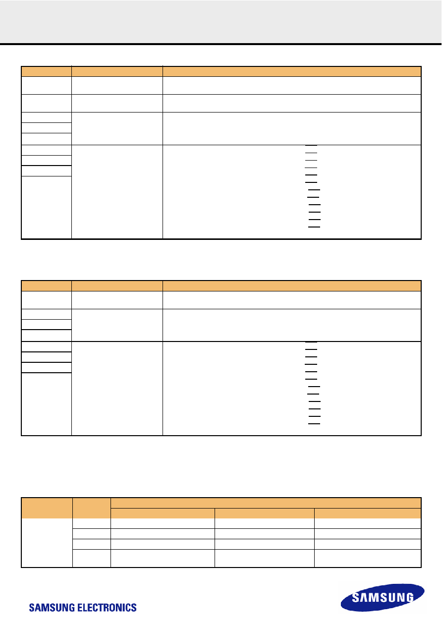
[Table 10] Burst Mode Configuration Register Table : K8S54(55)15ET(B)(Z)C : 66/83/108/133Mhz with the Sync MRS option
NOTE :
Initial wait state should be set according to it’s clock frequency. Table 10 recommend the program wait state for each clock frequencies.
Not 100% tested
[Table 11] Burst Mode Configuration Register Table : K8S56(57)15ET(B)(Z)C : 66/83/108/133Mhz with no option
NOTE :
Initial wait state should be set according to it’s clock frequency. Table 11 recommend the program wait state for each clock frequencies.
Not 100% tested
[Table 12] Burst Address Sequences
Address Bit
Function
Settings(Binary)
A19
Read Mode
1 = Synchronous Burst Read Mode
0 = Asynchronous Read Mode (default)
A18
RDY Active
1 = RDY active one clock cycle before data
0 = RDY active with data(default)
A17
Burst Read Mode
000 = Continuous(default)
001 = 8-word linear with wrap
010 = 16-word linear with wrap
011~111 = Reserve
A16
A15
A14
Programmable Wait State
0000 = Data is valid on the 4th active CLK edge after AVD transition to VIH
0001 = Data is valid on the 5th active CLK edge after AVD transition to VIH (40Mhz*)
0010 = Data is valid on the 6th active CLK edge after AVD transition to VIH (50/54Mhz*)
0011 = Data is valid on the 7th active CLK edge after AVD transition to VIH (60/66Mhz*)
0100 = Data is valid on the 8th active CLK edge after AVD transition to VIH (70Mhz*)
0101 = Data is valid on the 9th active CLK edge after AVD transition to VIH (80/83Mhz*)
0110 = Data is valid on the 10th active CLK edge after AVD transition to VIH (90/100Mhz*)
0111 = Data is valid on the 11th active CLK edge after AVD transition to VIH (108/110Mhz*)
1000 = Data is valid on the 12th active CLK edge after AVD transition to VIH (120Mhz*)
1001 = Data is valid on the 13th active CLK edge after AVD transition to VIH (133Mhz*,default)
1010 = Data is valid on the 14th active CLK edge after AVD transition to VIH
1011 = Data is valid on the 15th active CLK edge after AVD transition to VIH
A13
A12
A11
Address Bit
Function
Settings(Binary)
A18
RDY Active
1 = RDY active one clock cycle before data
0 = RDY active with data(default)
A17
Burst Read Mode
000 = Continuous(default)
001 = 8-word linear with wrap
010 = 16-word linear with wrap
011~111 = Reserve
A16
A15
A14
Programmable Wait State
0000 = Data is valid on the 4th active CLK edge after AVD transition to VIH
0001 = Data is valid on the 5th active CLK edge after AVD transition to VIH (40Mhz*)
0010 = Data is valid on the 6th active CLK edge after AVD transition to VIH (50/54Mhz*)
0011 = Data is valid on the 7th active CLK edge after AVD transition to VIH (60/66Mhz*)
0100 = Data is valid on the 8th active CLK edge after AVD transition to VIH (70Mhz*)
0101 = Data is valid on the 9th active CLK edge after AVD transition to VIH (80/83Mhz*)
0110 = Data is valid on the 10th active CLK edge after AVD transition to VIH (90/100Mhz*)
0111 = Data is valid on the 11th active CLK edge after AVD transition to VIH (108/110Mhz*)
1000 = Data is valid on the 12th active CLK edge after AVD transition to VIH (120Mhz*)
1001 = Data is valid on the 13th active CLK edge after AVD transition to VIH (133Mhz*,default)
1010 = Data is valid on the 14th active CLK edge after AVD transition to VIH
1011 = Data is valid on the 15th active CLK edge after AVD transition to VIH
A13
A12
A11
Start
Addr.
Burst Address Sequence
Continuous Burst
8-word Burst
16-word Burst
Wrap
0
0-1-2-3-4-5-6...
0-1-2-3-4-5-6-7
0-1-2-3 ... -D-E-F
1
1-2-3-4-5-6-7...
1-2-3-4-5-6-7-0
1-2-3-4 ... -E-F-0
2
2-3-4-5-6-7-8...
2-3-4-5-6-7-0-1
2-3-4-5 ... -F-0-1
.
相關(guān)PDF資料 |
PDF描述 |
|---|---|
| K9E2G08U0M-YIB00 | 256M X 8 FLASH 2.7V PROM, 30 ns, PDSO48 |
| KA-59-281 | TNC CONNECTOR, PLUG |
| KA-91-02 | RF STRAIGHT ADAPTER |
| KA-91-16 | RF TEE ADAPTER |
| KA-99-24 | RF STRAIGHT ADAPTER |
相關(guān)代理商/技術(shù)參數(shù) |
參數(shù)描述 |
|---|---|
| K8S5615ETC | 制造商:SAMSUNG 制造商全稱:Samsung semiconductor 功能描述:256Mb C-die NOR Flash |
| K8S6415EBB-DC7C | 制造商:SAMSUNG 制造商全稱:Samsung semiconductor 功能描述:64M Bit (4M x16) Muxed Burst , Multi Bank NOR Flash Memory |
| K8S6415EBB-DE7C | 制造商:SAMSUNG 制造商全稱:Samsung semiconductor 功能描述:64M Bit (4M x16) Muxed Burst , Multi Bank NOR Flash Memory |
| K8S6415EBB-FC7C | 制造商:SAMSUNG 制造商全稱:Samsung semiconductor 功能描述:64M Bit (4M x16) Muxed Burst , Multi Bank NOR Flash Memory |
| K8S6415EBB-FE7C | 制造商:SAMSUNG 制造商全稱:Samsung semiconductor 功能描述:64M Bit (4M x16) Muxed Burst , Multi Bank NOR Flash Memory |
發(fā)布緊急采購,3分鐘左右您將得到回復(fù)。