- 您現(xiàn)在的位置:買賣IC網(wǎng) > PDF目錄379208 > ICY7C1362C-166BGXI (CYPRESS SEMICONDUCTOR CORP) 9-Mbit (256K x 36/512K x 18) Pipelined SRAM PDF資料下載
參數(shù)資料
| 型號: | ICY7C1362C-166BGXI |
| 廠商: | CYPRESS SEMICONDUCTOR CORP |
| 元件分類: | DRAM |
| 英文描述: | 9-Mbit (256K x 36/512K x 18) Pipelined SRAM |
| 中文描述: | 512K X 18 CACHE SRAM, 3.5 ns, PBGA119 |
| 封裝: | 14 X 22 MM, 2.40 MM HEIGHT, LEAD FREE, PLASTIC, BGA-119 |
| 文件頁數(shù): | 12/31頁 |
| 文件大小: | 432K |
| 代理商: | ICY7C1362C-166BGXI |
第1頁第2頁第3頁第4頁第5頁第6頁第7頁第8頁第9頁第10頁第11頁當(dāng)前第12頁第13頁第14頁第15頁第16頁第17頁第18頁第19頁第20頁第21頁第22頁第23頁第24頁第25頁第26頁第27頁第28頁第29頁第30頁第31頁
PRELIMINARY
CY7C1360C
CY7C1362C
Document #: 38-05540 Rev. *C
Page 12 of 31
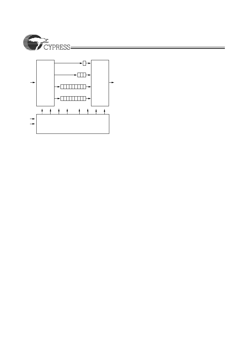
TAP Controller Block Diagram
Performing a TAP Reset
A RESET is performed by forcing TMS HIGH (V
DD
) for five
rising edges of TCK. This RESET does not affect the operation
of the SRAM and may be performed while the SRAM is
operating.
At power-up, the TAP is reset internally to ensure that TDO
comes up in a High-Z state.
TAP Registers
Registers are connected between the TDI and TDO balls and
allow data to be scanned into and out of the SRAM test
circuitry. Only one register can be selected at a time through
the instruction register. Data is serially loaded into the TDI ball
on the rising edge of TCK. Data is output on the TDO ball on
the falling edge of TCK.
Instruction Register
Three-bit instructions can be serially loaded into the instruction
register. This register is loaded when it is placed between the
TDI and TDO balls as shown in the Tap Controller Block
Diagram. Upon power-up, the instruction register is loaded
with the IDCODE instruction. It is also loaded with the IDCODE
instruction if the controller is placed in a reset state as
described in the previous section.
When the TAP controller is in the Capture-IR state, the two
least significant bits are loaded with a binary “01” pattern to
allow for fault isolation of the board-level serial test data path.
Bypass Register
To save time when serially shifting data through registers, it is
sometimes advantageous to skip certain chips. The bypass
register is a single-bit register that can be placed between the
TDI and TDO balls. This allows data to be shifted through the
SRAM with minimal delay. The bypass register is set LOW
(V
SS
) when the BYPASS instruction is executed.
Boundary Scan Register
The boundary scan register is connected to all the input and
bidirectional balls on the SRAM.
The boundary scan register is loaded with the contents of the
RAM I/O ring when the TAP controller is in the Capture-DR
state and is then placed between the TDI and TDO balls when
the controller is moved to the Shift-DR state. The EXTEST,
SAMPLE/PRELOAD and SAMPLE Z instructions can be used
to capture the contents of the I/O ring.
The Boundary Scan Order tables show the order in which the
bits are connected. Each bit corresponds to one of the bumps
on the SRAM package. The MSB of the register is connected
to TDI and the LSB is connected to TDO.
Identification (ID) Register
The ID register is loaded with a vendor-specific, 32-bit code
during the Capture-DR state when the IDCODE command is
loaded in the instruction register. The IDCODE is hardwired
into the SRAM and can be shifted out when the TAP controller
is in the Shift-DR state. The ID register has a vendor code and
other information described in the Identification Register
Definitions table.
TAP Instruction Set
Overview
Eight different instructions are possible with the three-bit
instruction register. All combinations are listed in the
Instruction Codes table. Three of these instructions are listed
as RESERVED and should not be used. The other five instruc-
tions are described in detail below.
The TAP controller used in this SRAM is not fully compliant to
the 1149.1 convention because some of the mandatory 1149.1
instructions are not fully implemented.
The TAP controller cannot be used to load address data or
control signals into the SRAM and cannot preload the I/O
buffers. The SRAM does not implement the 1149.1 commands
EXTEST or INTEST or the PRELOAD portion of
SAMPLE/PRELOAD; rather, it performs a capture of the I/O
ring when these instructions are executed.
Instructions are loaded into the TAP controller during the
Shift-IR state when the instruction register is placed between
TDI and TDO. During this state, instructions are shifted
through the instruction register through the TDI and TDO balls.
To execute the instruction once it is shifted in, the TAP
controller needs to be moved into the Update-IR state.
EXTEST
EXTEST is a mandatory 1149.1 instruction which is to be
executed whenever the instruction register is loaded with all
0s. EXTEST is not implemented in this SRAM TAP controller,
and therefore this device is not compliant to 1149.1. The TAP
controller does recognize an all-0 instruction.
When an EXTEST instruction is loaded into the instruction
register, the SRAM responds as if a SAMPLE/PRELOAD
instruction has been loaded. There is one difference between
the two instructions. Unlike the SAMPLE/PRELOAD
instruction, EXTEST places the SRAM outputs in a High-Z
state.
IDCODE
The IDCODE instruction causes a vendor-specific, 32-bit code
to be loaded into the instruction register. It also places the
instruction register between the TDI and TDO balls and allows
the IDCODE to be shifted out of the device when the TAP
controller enters the Shift-DR state.
Bypass Register
0
Instruction Register
0
1
2
Identification Register
0
1
2
29
30
31
.
.
.
Boundary Scan Register
0
1
2
.
.
x
.
.
.
S
election
Circuitr
y
Selection
Circuitry
TCK
TMS
TAP CONTROLLER
TDI
TDO
相關(guān)PDF資料 |
PDF描述 |
|---|---|
| ID100 | MONOLITHIC DUAL PICO AMPERE DIODES |
| ID100 | SCRs .5 Amp, Planar |
| IDT101494S7C | HIGH-SPEED BiCMOS ECL STATIC RAM 64K (16K】4-BIT) SRAM |
| IDT100494 | HIGH-SPEED BiCMOS ECL STATIC RAM 64K (16K】4-BIT) SRAM |
| IDT100494S10C | HIGH-SPEED BiCMOS ECL STATIC RAM 64K (16K】4-BIT) SRAM |
相關(guān)代理商/技術(shù)參數(shù) |
參數(shù)描述 |
|---|---|
| ICY7C1362C-166BZI | 制造商:CYPRESS 制造商全稱:Cypress Semiconductor 功能描述:9-Mbit (256K x 36/512K x 18) Pipelined SRAM |
| ICY7C1367B-166BGI | 制造商:CYPRESS 制造商全稱:Cypress Semiconductor 功能描述:9-Mb (256K x 36/512K x 18) Pipelined DCD Sync SRAM |
| ICY7C1373C-100BGI | 制造商:CYPRESS 制造商全稱:Cypress Semiconductor 功能描述:18-Mbit (512K x 36/1M x 18) Flow-Through SRAM with NoBL Architecture |
| ICY7C1373D-100BGI | 制造商:CYPRESS 制造商全稱:Cypress Semiconductor 功能描述:18-Mbit (512K x 36/1M x 18) Flow-Through SRAM with NoBLTM Architecture |
| ICY7C1373D-100BGXI | 制造商:CYPRESS 制造商全稱:Cypress Semiconductor 功能描述:18-Mbit (512K x 36/1M x 18) Flow-Through SRAM with NoBLTM Architecture |
發(fā)布緊急采購,3分鐘左右您將得到回復(fù)。