- 您現(xiàn)在的位置:買賣IC網(wǎng) > PDF目錄224000 > HYB18T1G800C4F-3 (QIMONDA AG) 128M X 8 DDR DRAM, 0.45 ns, PBGA60 PDF資料下載
參數(shù)資料
| 型號: | HYB18T1G800C4F-3 |
| 廠商: | QIMONDA AG |
| 元件分類: | DRAM |
| 英文描述: | 128M X 8 DDR DRAM, 0.45 ns, PBGA60 |
| 封裝: | GREEN, PLASTIC, TFBGA-60 |
| 文件頁數(shù): | 37/58頁 |
| 文件大小: | 1898K |
| 代理商: | HYB18T1G800C4F-3 |
第1頁第2頁第3頁第4頁第5頁第6頁第7頁第8頁第9頁第10頁第11頁第12頁第13頁第14頁第15頁第16頁第17頁第18頁第19頁第20頁第21頁第22頁第23頁第24頁第25頁第26頁第27頁第28頁第29頁第30頁第31頁第32頁第33頁第34頁第35頁第36頁當(dāng)前第37頁第38頁第39頁第40頁第41頁第42頁第43頁第44頁第45頁第46頁第47頁第48頁第49頁第50頁第51頁第52頁第53頁第54頁第55頁第56頁第57頁第58頁
HYB18T1G[40/80/16]0C4F
1-Gbit Double-Data-Rate-Two SDRAM
Internet Data Sheet
Rev. 1.01, 2008-11
42
04212008-66HT-ZLFE
1)
V
DDQ = 1.8 V ± 0.1V; VDD = 1.8 V ± 0.1 V.
2) Timing that is not specified is illegal and after such an event, in order to guarantee proper operation, the DRAM must be powered down
and then restarted through the specified initialization sequence before normal operation can continue.
3) Timings are guaranteed with CK/CK differential Slew Rate of 2.0 V/ns. For DQS signals timings are guaranteed with a differential Slew
Rate of 2.0 V/ns in differential strobe mode and a Slew Rate of 1 V/ns in single ended mode.
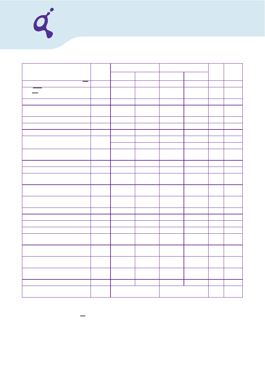
DQ low impedance time from CK/CK
t
LZ.DQ
2×
t
AC.MIN
t
AC.MAX
2×
t
AC.MIN
t
AC.MAX
ps
DQS/DQS low-impedance time from
CK / CK
t
LZ.DQS
t
AC.MIN
t
AC.MAX
t
AC.MIN
t
AC.MAX
ps
MRS command to ODT update delay
t
MOD
0
12
0
12
ns
Mode register set command cycle
time
t
MRD
2—
nCK
OCD drive mode output delay
t
OIT
0
12
0
12
ns
DQ/DQS output hold time from DQS
t
QH
t
HP – tQHS
—
t
HP – tQHS
—ps
DQ hold skew factor
t
QHS
—
300
—
340
ps
Average periodic refresh Interval
t
REFI
—7.8
μs
—3.9
μs
Auto-Refresh to Active/Auto-Refresh
command period
t
RFC
127.5
—
127.5
—
ns
Read preamble
t
RPRE
0.9
1.1
0.9
1.1
t
CK.AVG
Read postamble
t
RPST
0.4
0.6
0.4
0.6
t
CK.AVG
Active to active command period for
1KB page size products
t
RRD
7.5
—
7.5
—
ns
Active to active command period for
2KB page size products
t
RRD
10
—
10
—
ns
Internal Read to Precharge command
delay
t
RTP
7.5
—
7.5
—
ns
Write preamble
t
WPRE
0.35
—
0.35
—
t
CK.AVG
Write postamble
t
WPST
0.4
0.6
0.4
0.6
t
CK.AVG
Write recovery time
t
WR
15
—
15
—
ns
Internal write to read command delay
t
WTR
7.5
—
7.5
—
ns
Exit active power down to read
command
t
XARD
2—
nCK
Exit active power down to read
command (slow exit, lower power)
t
XARDS
8 – AL
—
7 – AL
—
nCK
Exit precharge power-down to any
command
t
XP
2—
nCK
Exit self-refresh to a non-read
command
t
XSNR
t
RFC +10
—
t
RFC +10
—
ns
Exit self-refresh to read command
t
XSRD
200
—
200
—
nCK
Write command to DQS associated
clock edges
WL
RL – 1
RL–1
nCK
Parameter
Symbol
DDR2–800
DDR2–667
Unit
Note1)2)3
)4)5)6)7)
Min.
Max.
Min.
Max.
相關(guān)PDF資料 |
PDF描述 |
|---|---|
| HYB3165800AJ-40 | 8M X 8 FAST PAGE DRAM, 40 ns, PDSO32 |
| HYB39S64400AT-8 | 16M X 4 SYNCHRONOUS DRAM, 6 ns, PDSO54 |
| HYC532410-50 | 4M X 32 MULTI DEVICE DRAM CARD, 50 ns, XMA88 |
| HYE18M256320CF-7.5 | 8M X 32 DDR DRAM, 6 ns, PBGA90 |
| HYM564124AR-60 | 1M X 64 EDO DRAM MODULE, DMA168 |
相關(guān)代理商/技術(shù)參數(shù) |
參數(shù)描述 |
|---|---|
| HYB18T256400AF-3.7 | 制造商:Infineon Technologies AG 功能描述:64M X 4 DDR DRAM, 0.5 ns, PBGA60 |
| HYB18T256400AF-5 | 制造商:Infineon Technologies AG 功能描述:SDRAM, DDR, 64M x 4, 60 Pin, Plastic, BGA |
| HYB18T256800AF-5 | 制造商:Infineon Technologies AG 功能描述: |
| HYB18T512161BF-25 | 制造商:Qimonda 功能描述:SDRAM, DDR, 32M x 16, 84 Pin, Plastic, BGA |
| HYB18T512400AF-5 | 制造商:Intersil Corporation 功能描述:SDRAM, DDR, 128M x 4, 60 Pin, Plastic, BGA |
發(fā)布緊急采購,3分鐘左右您將得到回復(fù)。