- 您現(xiàn)在的位置:買賣IC網(wǎng) > PDF目錄383075 > HSP50214B (Intersil Corporation) Programmable Downconverter PDF資料下載
參數(shù)資料
| 型號: | HSP50214B |
| 廠商: | Intersil Corporation |
| 英文描述: | Programmable Downconverter |
| 中文描述: | 可編程變頻器 |
| 文件頁數(shù): | 32/60頁 |
| 文件大?。?/td> | 573K |
| 代理商: | HSP50214B |
第1頁第2頁第3頁第4頁第5頁第6頁第7頁第8頁第9頁第10頁第11頁第12頁第13頁第14頁第15頁第16頁第17頁第18頁第19頁第20頁第21頁第22頁第23頁第24頁第25頁第26頁第27頁第28頁第29頁第30頁第31頁當(dāng)前第32頁第33頁第34頁第35頁第36頁第37頁第38頁第39頁第40頁第41頁第42頁第43頁第44頁第45頁第46頁第47頁第48頁第49頁第50頁第51頁第52頁第53頁第54頁第55頁第56頁第57頁第58頁第59頁第60頁
3-32
The Discriminator FIR filter input selections are made in
Control Word 27, Bits 18 and 19. The bit definitions are:
00 Item (1) described above.
01 Item (2) described above.
1X Item (3) described above.
Control Word 27, Bit 14 is used to control the Q input to the
coordinate converter. The bit definitions is:
0
1
I and Q enabled to the I/Q to R/Theta block.
The Q input to the I/Q to R/Theta block is zeroed.
The enable signals associated with the various input
selections to the Discriminator FIR filter are:
1
The data ready strobe from the coordinate con-
verter block.
The data ready strobe from the coordinate con-
verter block.
The enable signals associated with the various input
selections to the coordinate converter are:
2
3a
The data ready signal to the coordinate converter
block when the resampler is bypassed. This is the
AGC output data ready signal.
The data ready to the coordinate converter block
when the resampler/halfband filters are enabled.
This is the resampler halfband filter block output
data ready signal.
The discriminator input is 18 bits, and the output is rounded
asymmetrically to 16 bits. The phase into the discriminator
can be multiplied by 2
0
, 2
1
, 2
2
, or 2
3
(modulo 2
π
) to remove
PSK data modulation. All programmable parameters for the
Frequency Discriminator are set in Control Word 17. Bits 15
and 16 are the phase multiplier which represents the shift
applied to the input phase. For CW, the multiply should equal
2
0
, (00). For BPSK, QPSK, and 8PSK, the multiply should
equal 2
1
, (01); 2
2
, (10); or 2
3
, (11); respectively. Bit 14 is
used to enable or disable the discriminator. Bits 11-13 set
the decimation in the programmable FIR filter. Bit 10 sets the
filter symmetry type as either odd or even, bit 9 sets whether
the filter is asymmetric or symmetric, and bits 3-8 set the
number of FIR filter taps. Bits 0-2 set the number of delays in
the frequency discriminator.
3b
Output Section
The Output Section routes the 7 types of processed signals to
output pins in three basic modes. These basic modes are:
Parallel Direct Output, Serial Direct Output, and the Buffer
RAM Output. The Serial and Parallel Direct Output modes
were designed to output data strobes and “real time”
continuous streams of data. The Buffer RAM Output mode
outputs data upon receipt of an asynchronous request from
an external DSP processor or other baseband processing
engine. The use of the interrupt signal from the
Programmable Down Converter in conjunction with the
request strobes from the controller ensures that data is
transferred only when both the controller and the
Programmable Down Converter are ready. The Buffer RAM
output can be operated in a First In First Out (FIFO) or
SNAPSHOT mode with the data output either via the 8-bit
processor interface or a 16-bit processor interface.
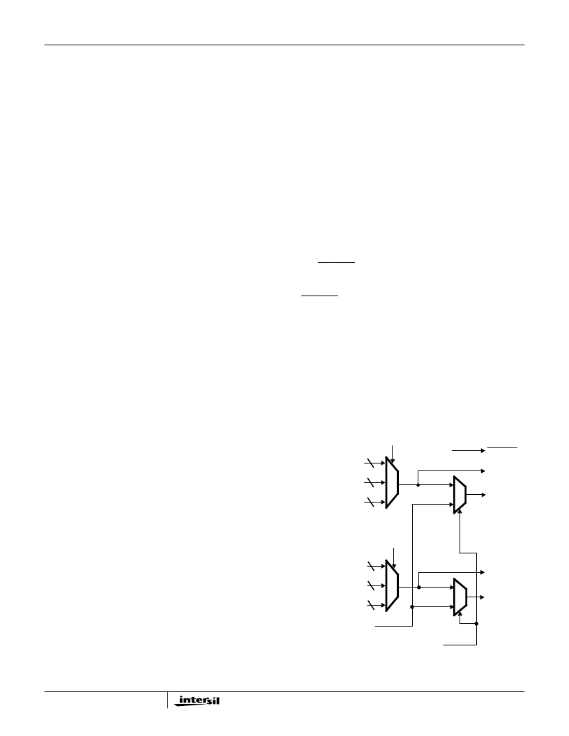
Parallel Direct Output Port Mode
The Parallel Direct Output Port Mode outputs two 16-bit words,
AOUT and BOUT, of “real time” data. Figure 30 details the
parallel output circuitry. Selection of the data source for the
AOUT and BOUT parallel outputs is done via Control Word 20,
Bits 22-23, and 20-21, respectively. The AOUT port can output
I, Magnitude, or Frequency data. The BOUT port can output Q,
Phase or Magnitude data. The upper bytes of AOUT and
BOUT are always in the paralleldirect mode.The 16-bit parallel
direct mode is selected by setting Control Word 20, Bit 25, to
zero.
The DATARDY output is asserted during the first clock cycle
of the new data on the AOUT bus. The rate at which the data
out of the HSP50214 transitions and the rate at which
DATARDY is asserted can be different.
Data Transitions:
The transition rate of the parallel output data is dependent on
which of the three types of data is selected for the AOUT
Output channel: I (real symbols), |r| (magnitude), or f
(frequency). Q (quadrature symbols), (phase), or |r|
(magnitude) are available on the BOUT output. When selected
as an output, the I Q, |r|, and outputs transition at the symbol
rate. The f (frequency) output transitions at the discriminator
FIR filter output rate.
M
M
I
MAG
FREQ
Q
PHAS
MAG
AOUT(15:8)
A(7:0)
M
RAM(15:8)
AOUT(7:0)
B(7:0)
M
BOUT(7:0)
RAM (7:0)
16
16
16
16
16
16
BOUT DIRECT PAR
OUTPUT MODE
DATA SOURCE
AOUT DIRECT PAR
OUTPUT MODE
DATA SOURCE
DATA SOURCE FOR LSB
BOUT(15:8)
B(15:8)
A(15:8)
RAM (15:0)
Controlled via microprocessor interface.
FIGURE 30. PARALLEL OUTPUT BLOCK DIAGRAM
DATARDY
(2’s COMPLEMENT)
(UNSIGNED BINARY)
(2’s COMPLEMENT)
(2’s COMPLEMENT)
(2’s COMPLEMENT)
(UNSIGNED BINARY)
HSP50214B
相關(guān)PDF資料 |
PDF描述 |
|---|---|
| HSP50214BVC | Programmable Downconverter |
| HSP50214BVI | Programmable Downconverter |
| HT84 | ADSL Coupling Transformers |
| HT84-00594 | ADSL Coupling Transformers |
| HT8400594S | ADSL Coupling Transformers |
相關(guān)代理商/技術(shù)參數(shù) |
參數(shù)描述 |
|---|---|
| HSP50214B_07 | 制造商:INTERSIL 制造商全稱:Intersil Corporation 功能描述:Programmable Downconverter |
| HSP50214BVC | 功能描述:上下轉(zhuǎn)換器 120L MQFP COMTEMP 14-BIT PROGRAMMABLE DOWNCONVERTER 65MSPS RoHS:否 制造商:Texas Instruments 產(chǎn)品:Down Converters 射頻:52 MHz to 78 MHz 中頻:300 MHz LO頻率: 功率增益: P1dB: 工作電源電壓:1.8 V, 3.3 V 工作電源電流:120 mA 最大功率耗散:1 W 最大工作溫度:+ 85 C 安裝風(fēng)格:SMD/SMT 封裝 / 箱體:PQFP-128 |
| HSP50214BVCZ | 功能描述:上下轉(zhuǎn)換器 120L MQFP COMTEMP 14-BIT PROG DWNCNVRT RoHS:否 制造商:Texas Instruments 產(chǎn)品:Down Converters 射頻:52 MHz to 78 MHz 中頻:300 MHz LO頻率: 功率增益: P1dB: 工作電源電壓:1.8 V, 3.3 V 工作電源電流:120 mA 最大功率耗散:1 W 最大工作溫度:+ 85 C 安裝風(fēng)格:SMD/SMT 封裝 / 箱體:PQFP-128 |
| HSP50214BVI | 功能描述:上下轉(zhuǎn)換器 120L MQFP INDTEMP 14-BIT PROGRAMMABLE DOWNCONVERTER 65MSPS RoHS:否 制造商:Texas Instruments 產(chǎn)品:Down Converters 射頻:52 MHz to 78 MHz 中頻:300 MHz LO頻率: 功率增益: P1dB: 工作電源電壓:1.8 V, 3.3 V 工作電源電流:120 mA 最大功率耗散:1 W 最大工作溫度:+ 85 C 安裝風(fēng)格:SMD/SMT 封裝 / 箱體:PQFP-128 |
| HSP50214BVIZ | 功能描述:上下轉(zhuǎn)換器 120L MQFP INDTEMP 14-BIT PROG DWNCNVRT RoHS:否 制造商:Texas Instruments 產(chǎn)品:Down Converters 射頻:52 MHz to 78 MHz 中頻:300 MHz LO頻率: 功率增益: P1dB: 工作電源電壓:1.8 V, 3.3 V 工作電源電流:120 mA 最大功率耗散:1 W 最大工作溫度:+ 85 C 安裝風(fēng)格:SMD/SMT 封裝 / 箱體:PQFP-128 |
發(fā)布緊急采購,3分鐘左右您將得到回復(fù)。