- 您現(xiàn)在的位置:買賣IC網(wǎng) > PDF目錄371898 > HSP50016-EV (Intersil Corporation) DDC Evaluation Platform PDF資料下載
參數(shù)資料
| 型號: | HSP50016-EV |
| 廠商: | Intersil Corporation |
| 英文描述: | DDC Evaluation Platform |
| 中文描述: | DDC的評估平臺 |
| 文件頁數(shù): | 21/31頁 |
| 文件大小: | 209K |
| 代理商: | HSP50016-EV |
第1頁第2頁第3頁第4頁第5頁第6頁第7頁第8頁第9頁第10頁第11頁第12頁第13頁第14頁第15頁第16頁第17頁第18頁第19頁第20頁當前第21頁第22頁第23頁第24頁第25頁第26頁第27頁第28頁第29頁第30頁第31頁

3-218
HSP50016 supports two types of testing. Control Word 7 can
be used to verify the operation of the circuit through the
divide and conquer method. Setting the Enable Test Bit
(Control Word 1, Bit 3) equal to a 1 enables the test features
controlled by Control Word 7. (This bit is in Control Word 1
so that Word 7 does not have to be loaded if the test features
are not being used.) The functions allowed by Control Word 7
are shown in Table 10.
NOTE: Asserting bits 9 and 13 of Control Word 7 will put
all outputs to a static mode. This may remove strobe
enables or clocks used to read the data signals. This Test
Mode was intended for interface evaluation at the board
level.
The DDC also has a Test Access Port (TAP). This port is
fully conformant to IEEE Std. 1149.1 - 1990 - IEEE Standard
Test Access Port and Boundary-Scan [2]. The TAP supports
the following instructions: BYPASS, SAMPLE/PRELOAD,
INTEST, EXTEST, RUNBIST and IDCODE. In addition, there
are seven instructions called RDCNTLWD1-7, which read
the contents of the control words over the TAP. The address
bits and bit 36 are only used to determine the destination of
data during loading; they are not stored, so they are not read
out with the RDCNTLWD1-7 instruction.
Summary
To use the DDC in a down conversion application three items
must be considered and designed to compliance. Solutions
must satisfy all three items.
1. The Nyquist Sampling Rate for the bandwidth of interest
F
S
≥
2BW, where BW is the bandwidth of interest.
2. ThecompositeFIR/HDFdoublesidedbandwidth,BW
-3dB
= 0.1375F
S
/R.
3. Thedesiredserialoutputclockrate(totaldecimation,plus
parallel to serial conversion rate increase).
NOTE:
R
FIR
= 2 for real mode, 4 for all other modes.
Applications
Down Conversion
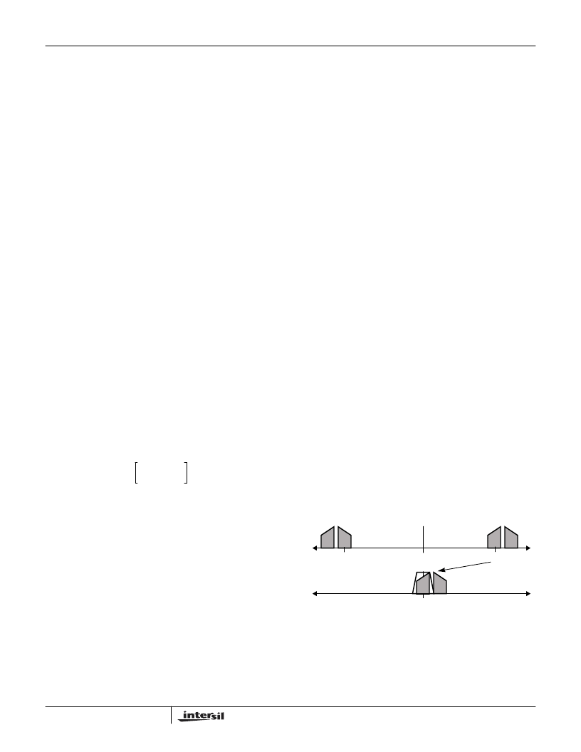
The primary spectral operation in the DDC is down
conversion of an input signal to base band, see Figure 15.
This process is done in two steps: multiplication of the input
waveform by an internally generated quadrature sinusoid,
i.e., modulation and lowpass filtering to attenuate the
unwanted spectral components. The unwanted spectral
components have two sources, the input signal and an
artifact of the modulation process.
The modulation process can be written as:
u(n) = x(n)e
-j
ω
c = x(n)[cos(
ω
c
) - jsin(
ω
c
)]
Where x(n) is the real input data sequence,
ω
= 2
π
f, and
ω
c
is
the frequency of the signal generated by the SIN/COS
Generator.
For demonstration purposes let x(n) = cos(
ω
k
n). The
multiplication then becomes:
The signal u(n) is passed through a low pass filter; assuming
that the filter passes the low frequency terms with no
degradation and attenuates the high frequency terms
completely, the filtering operation produces the output:
When the magnitude of the input signal x(n) is one, the
magnitude of v(n) is 1/2. Both the I and Q channels are
multiplied by a factor of two to yield:
Figure 16 shows an HSP50016 in a single channel down
conversion circuit. Notice that the input data is only 12 bits,
so it is justified to the MSB of the DDC’s input data. If a
smaller sample width is used, it is recommended that the
MSB of the data is input into DATA15. The unused bits are
connected to ground. This alignment makes it easier to
locate the position of the MSB in the output data. Note that
the input is configured for offset binary arithmetic and the
output is set up for I followed by Q, which enables the use of
only one serial connection to the output processor. The
serial data clock of the processor and the Control Clock of
the DDC are driven by a TTL compatible oscillator. (IQCLK
cannot be used for this purpose since its frequency is
indeterminate until the DDC has been configured). Note that
many processors provide a bit clock which eliminates the
need for the external oscillator.
IQCLK Frequency
f
Length
FIR
)
-----------------------------------
1
–
=
(EQ. 17)
u(n) = cos(
ω
k
n)[cos(
ω
c
n) - jsin(
ω
c
n)]
= 1/2[cos((
ω
k
-
ω
c
)n) + cos((
ω
k
+
ω
c
)n)
- j(sin((
ω
k
+
ω
c
)n) - sin((
ω
k
-
ω
c
)n))]
(EQ. 18)
v(n) = 1/2(cos((
ω
k
-
ω
c
)n) + jsin((
ω
k
-
ω
c
)n))
= 1/2e
j
(
ω
k
-
ω
c)
n
(EQ. 19)
w(n) = cos((
ω
k
-
ω
c
)n) + jsin((
ω
k
-
ω
c
)n)
= e
j(
ω
k
-
ω
c
)n
.
(EQ. 20)
ω
C
-
ω
C
A. INPUT SIGNAL SPECTRUM
B. DOWN CONVERSION AND FILTERING
FIGURE 15. DOWN CONVERSION
HSP50016
相關PDF資料 |
PDF描述 |
|---|---|
| HSP50016JC-52 | Digital Down Converter |
| HSP50016JC-75 | Digital Down Converter |
| HSP50110JC-60 | Communications Tuner Circuit |
| HSP50306SC-25 | Digital QPSK Demodulator |
| HSP50306SC-2596 | Digital QPSK Demodulator |
相關代理商/技術(shù)參數(shù) |
參數(shù)描述 |
|---|---|
| HSP50016GC-52 | 制造商:Rochester Electronics LLC 功能描述:- Bulk |
| HSP50016JC-52 | 功能描述:上下轉(zhuǎn)換器 DIGITAL DOWN CONVERTER 44 PLCC, 52MHZ, COMM RoHS:否 制造商:Texas Instruments 產(chǎn)品:Down Converters 射頻:52 MHz to 78 MHz 中頻:300 MHz LO頻率: 功率增益: P1dB: 工作電源電壓:1.8 V, 3.3 V 工作電源電流:120 mA 最大功率耗散:1 W 最大工作溫度:+ 85 C 安裝風格:SMD/SMT 封裝 / 箱體:PQFP-128 |
| HSP50016JC-5296 | 制造商:Rochester Electronics LLC 功能描述:TAPE AND REEL OF HSP50016JC-52 - Bulk |
| HSP50016JC-75 | 制造商:Rochester Electronics LLC 功能描述:DIGITAL DOWN CONVERTER 44 PLCC 75MHZ COMM - Bulk |
| HSP50016JI-52 | 制造商:Rochester Electronics LLC 功能描述:DIGITAL DOWN CONVERTER 44 PLCC, 52MHZ, COMM,INDS - Bulk |
發(fā)布緊急采購,3分鐘左右您將得到回復。