- 您現(xiàn)在的位置:買賣IC網(wǎng) > PDF目錄383032 > GS816236 (GSI TECHNOLOGY) 16Mb(512K x 36Bit)S/DCD Sync Burst SRAM(16M位(512K x 36位)可選單/雙循環(huán)取消同步?jīng)_靜態(tài)RAM(帶2位脈沖地址計(jì)數(shù)器)) PDF資料下載
參數(shù)資料
| 型號(hào): | GS816236 |
| 廠商: | GSI TECHNOLOGY |
| 英文描述: | 16Mb(512K x 36Bit)S/DCD Sync Burst SRAM(16M位(512K x 36位)可選單/雙循環(huán)取消同步?jīng)_靜態(tài)RAM(帶2位脈沖地址計(jì)數(shù)器)) |
| 中文描述: | 16Mb的(為512k × 36Bit)的S /雙氰胺同步突發(fā)靜態(tài)存儲(chǔ)器(1,600位(為512k × 36位)可選單/雙循環(huán)取消同步?jīng)_靜態(tài)隨機(jī)存儲(chǔ)器(帶2位脈沖地址計(jì)數(shù)器)) |
| 文件頁數(shù): | 26/38頁 |
| 文件大小: | 826K |
| 代理商: | GS816236 |
第1頁第2頁第3頁第4頁第5頁第6頁第7頁第8頁第9頁第10頁第11頁第12頁第13頁第14頁第15頁第16頁第17頁第18頁第19頁第20頁第21頁第22頁第23頁第24頁第25頁當(dāng)前第26頁第27頁第28頁第29頁第30頁第31頁第32頁第33頁第34頁第35頁第36頁第37頁第38頁
Rev: 2.10 11/2000
Specifications cited are subject to change without notice. For latest documentation see http://www.gsitechnology.com.
26/38
1999, Giga Semiconductor, Inc.
Preliminary
GS816218/36/72B-225/200/180/166/150/133
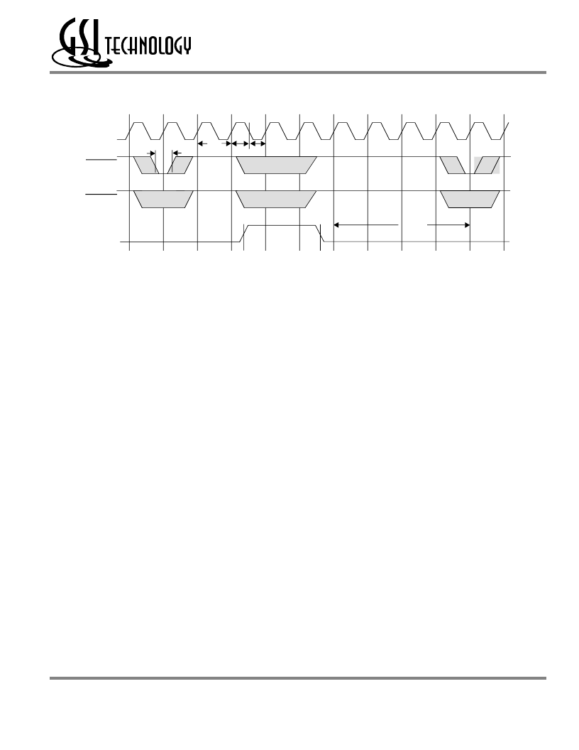
Sleep Mode Timing Diagram
Application Tips
Single and Dual Cycle Deselect
SCD devices force the use of “dummy read cycles” (read cycles that are launched normally, but that are ended with the output
drivers inactive) in a fully synchronous environment. Dummy read cycles waste performance, but their use usually assures there
will be no bus contention in transitions from reads to writes or between banks of RAMs. DCD SRAMs do not waste bandwidth on
dummy cycles and are logically simpler to manage in a multiple bank application (wait states need not be inserted at bank address
boundary crossings), but greater care must be exercised to avoid excessive bus contention.
JTAG Port Operation
Overview
The JTAG Port on this RAM operates in a manner consistent with IEEE Standard 1149.1-1990, a serial boundary scan interface
standard (commonly referred to as JTAG), but does not implement all of the functions required for 1149.1 compliance. Unlike
JTAG implementations that have been common among SRAM vendors for the last several years, this implementation does offer a
form of EXTEST, known as Clock Assisted EXTEST, reducing or eliminating the “hand coding” that has been required to
overcome the test program compiler errors caused by previous non-compliant implementations. The JTAG Port interfaces with
conventional 2.5 V CMOS logic level signaling.
Disabling the JTAG Port
It is possible to use this device without utilizing the JTAG port. The port is reset at power-up and will remain inactive unless
clocked. TCK, TDI, and TMS are designed with internal pull-up circuits.To assure normal operation of the RAM with the JTAG
Port unused, TCK, TDI, and TMS may be left floating or tied to either V
DD
or V
SS
. TDO should be left unconnected.
CK
ADSP
ADSC
tH
tKH tKL
tKC
tS
ZZ
tZZR
tZZH
tZZS
~
~
~
~
Snooze
相關(guān)PDF資料 |
PDF描述 |
|---|---|
| GS816272 | 16Mb(256K x 72Bit)S/DCD Sync Burst SRAM(16M位(256K x 72位)可選單/雙循環(huán)取消同步靜態(tài)RAM(帶2位脈沖地址計(jì)數(shù)器)) |
| GS8162Z18BGB-200I | 18Mb Pipelined and Flow Through Synchronous NBT SRAM |
| GS8162Z18BB | 18Mb Pipelined and Flow Through Synchronous NBT SRAM |
| GS8162Z18BB-150 | 18Mb Pipelined and Flow Through Synchronous NBT SRAM |
| GS8162Z18BB-150I | 18Mb Pipelined and Flow Through Synchronous NBT SRAM |
相關(guān)代理商/技術(shù)參數(shù) |
參數(shù)描述 |
|---|---|
| GS816236BB-150 | 制造商:GSI Technology 功能描述:SRAM SYNC QUAD 3.3V 18MBIT 512KX36 7.5NS/3.8NS 119FBGA - Trays |
| GS816236BB-150I | 制造商:GSI Technology 功能描述:SRAM SYNC QUAD 3.3V 18MBIT 512KX36 7.5NS/3.8NS 119FBGA - Trays |
| GS816236BB-150IV | 制造商:GSI Technology 功能描述:SRAM SYNC QUAD 2.5V/3.3V 18MBIT 512KX36 7.5NS/3.8NS 119FPBGA - Trays |
| GS816236BB-150V | 制造商:GSI Technology 功能描述:SRAM SYNC QUAD 2.5V/3.3V 18MBIT 512KX36 7.5NS/3.8NS 119FPBGA - Trays |
| GS816236BB-200 | 制造商:GSI Technology 功能描述:SRAM SYNC QUAD 3.3V 18MBIT 512KX36 6.5NS/3NS 119FBGA - Trays |
發(fā)布緊急采購,3分鐘左右您將得到回復(fù)。