- 您現(xiàn)在的位置:買賣IC網(wǎng) > PDF目錄378447 > CIP3250A (MICRONAS SEMICONDUCTOR HOLDING AG) Component Interface Processor PDF資料下載
參數(shù)資料
| 型號: | CIP3250A |
| 廠商: | MICRONAS SEMICONDUCTOR HOLDING AG |
| 元件分類: | 消費家電 |
| 英文描述: | Component Interface Processor |
| 中文描述: | SPECIALTY CONSUMER CIRCUIT, PQCC68 |
| 封裝: | PLASTIC, LCC-68 |
| 文件頁數(shù): | 15/44頁 |
| 文件大小: | 326K |
| 代理商: | CIP3250A |
第1頁第2頁第3頁第4頁第5頁第6頁第7頁第8頁第9頁第10頁第11頁第12頁第13頁第14頁當前第15頁第16頁第17頁第18頁第19頁第20頁第21頁第22頁第23頁第24頁第25頁第26頁第27頁第28頁第29頁第30頁第31頁第32頁第33頁第34頁第35頁第36頁第37頁第38頁第39頁第40頁第41頁第42頁第43頁第44頁
ADVANCE INFORMATION
CIP 3250A
15
Micronas
2.12.4. Orthogonal 4:1:1 Output Format
The orthogonal 4:1:1 output format is compatible to the
industry standard. The U and V samples are skew cor-
rected and interpolated to an orthogonal sampling raster
(see Table 2
–
8).
Table 2–8:
4:1:1 orthogonal output format
Luma
Chroma
Y
1
Y
2
Y
3
Y
4
C
3
, C
7
C
2
, C
6
C
1
, C
5
C
0
, C
4
U
17
U
16
V
17
V
16
U
15
U
14
V
15
V
14
U
13
U
12
V
13
V
12
U
11
U
10
V
11
V
10
Note:
U
xY
x = pixel number and y = bit number
2.12.5. YUV Output Levels
The Y output black level of the CIP 3250A can be con-
verted from ITU-R 601 Standard (digital 16) to DIGIT
2000
Standard
(digital
<16>ADD16Q.
32)
via
I
2
C
register
2.13. I/O Code Levels
–
ITU-R/DIGIT 3000 code levels:
Y or RGB = 16...240, clamp level = 16
UV =
±
112
,
bias level = 0
–
or DIGIT 2000 code levels:
Y = 32...127, clamp level = 32
UV =
±
127,
bias level = 0
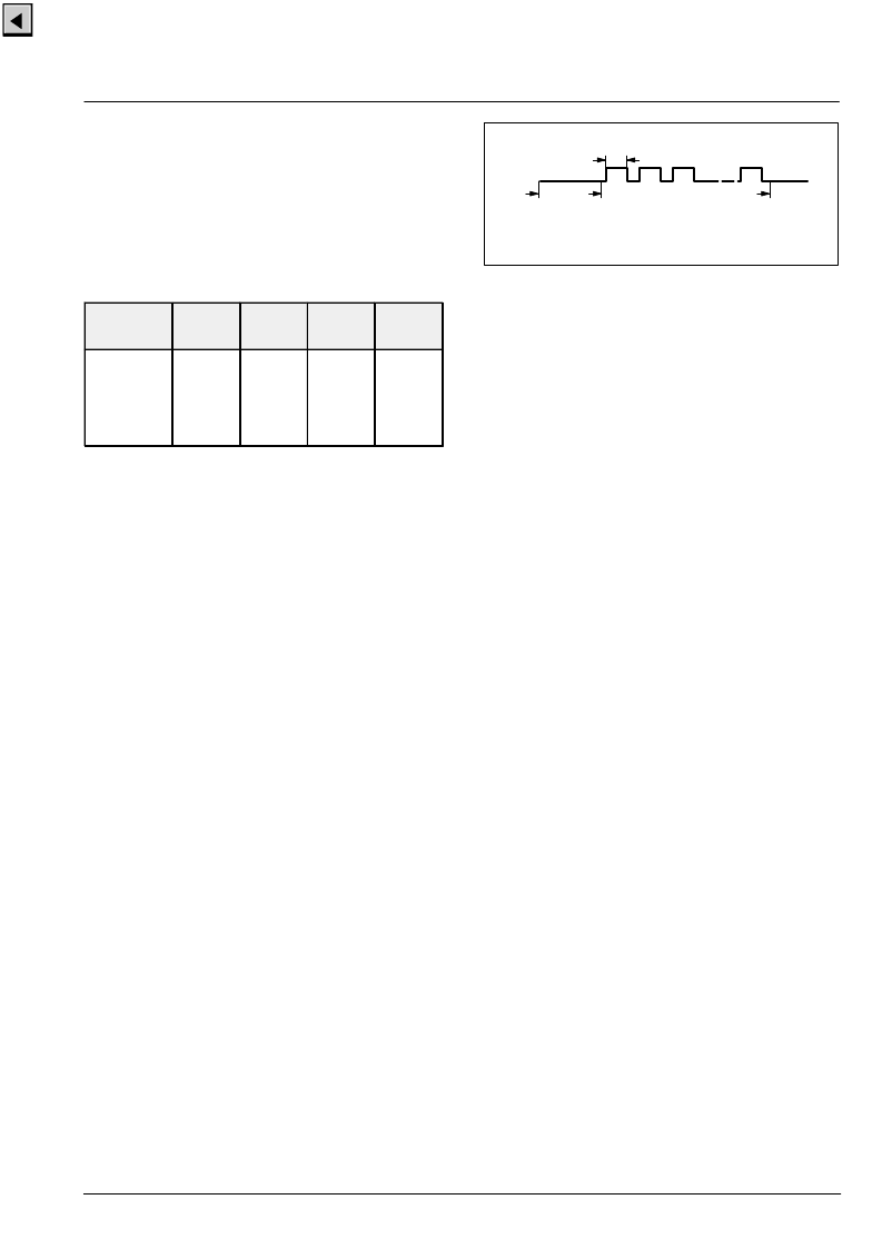
2.14. AVO Active Video Output
In a DIGIT 3000 system environment, the AVO signal is
equivalent to the delayed AVI signal. It signalizes valid
video data and chroma multiplex at the output of the
CIP 3250A. Furthermore, the AVO signal can be used to
control the write enable of a frame memory. The polarity
of the AVO signal is programmable via I
2
C register
<10>AVOINV.
In a DIGIT 2000 system environment, the AVO signal
can be programmed via I
2
C registers <23> to <26> to
define a window of valid video data at the output of the
CIP 3250A (see Fig. 2
–
11).
AVO
Fig. 2–11:
Programmable AVO signal
<23>AVHSTRT
<24>AVHLEN
<26>AVVSTOP
<25>AVVSTRT
start of field
Select the desired mode via I
2
C register <17>AVINT. If
the AVO signal is derived from the AVI signal, the I
2
C
registers <22>AVDLY can be used to compensate inter-
nal processing delays of the CIP 3250A.
I
2
C register <22>AVPR can be used to precede the AVO
signal in relation to the RGB/YUV data output up to 3
clocks.
2.15. PRIO Interface
–
real-time bus arbitration for 8 sources in DIGIT 3000
picture bus.
Up to eight digital YUV or RGB sources (main decoder,
PIP, OSD, Text, etc.) may be selected in real-time by
means of a 3 bit priority bus. Thus, a pixelwise bus arbi-
tration and source switching is possible. It is essential
that all YUV-sources are synchronous and orthogonal.
In general, each source (= master) has its own YUV bus
request. This bus request may either be software or
hardware controlled, i.e. a fast blank signal. Data colli-
sion is avoided by a bus arbiter that provides the individ-
ual bus acknowledge, in accordance to a user defined
priority.
Each master sends a bus request with its individual
priority ID onto the PRIO-bus and immediately reads
back the bus status. Only in case of positive arbitration
(send-PRIO-ID = read-PRIO-ID), the RGB/YUV outputs
become active and the data is send. PRIO requests
must be enabled by I
2
C register <14>PRIOEN.
The requests asserted by the CIP 3250A may be gener-
ated by two different sources, which are selectable by
I
2
C register <09>PRIOSRC. With the first source, the
CIP 3250A asserts requests only when the AVO signal
is active, else RGB/YUV outputs are tristated. With the
second source, the CIP 3250A asserts continuous re-
quests where the YUV data are forced to
“
clamp/bias
level data
”
(see section 2.13.) during the time that the
AVO signal is inactive.
If only one source is connected to the YUV bus, the out-
puts GL, RC, and B may drive the bus during a full clock
cycle. This can be selected by I
2
C register <06>HALF-
OUT. If more than one source is connected to the YUV
bus, the output drivers must be switched to driving only
during the first half of clock cycle to avoid bus collision.
In the last case, the layout of the PCB must consider that
相關PDF資料 |
PDF描述 |
|---|---|
| CJF6668 | PNP SILICON PLANAR DARLINGTON POWER TRANSISTOR |
| CL680 | SINGLE-CHIP AUDIO/VIDEO/CD-ROM DECODER WITH INTEGRATED NTSC/PAL ENCODER |
| CLA17 | 10 TO 1000 MHz TO-8 CASCADABLE LIMITING AMPLIFIER |
| CLC40 | Fllstandssensoren Schaltverstarker Baureihe CLC |
| CLC401AJE-TR13 | Current-Feedback Operational Amplifier |
相關代理商/技術(shù)參數(shù) |
參數(shù)描述 |
|---|---|
| CIP3542 | 制造商:CANOPUS 制造商全稱:CANOPUS 功能描述:Piezo Element |
| CIP3548 | 制造商:CANOPUS 制造商全稱:CANOPUS 功能描述:Piezo Element |
| CIPAW-C | 制造商:Panduit Corp 功能描述:PLASTIC SNAP-IN ICON WITH PHONE IMAGE 制造商:Panduit Corp 功能描述:PHONE ICON, ARCTIC WHITE - Bag |
| CIPBL-C | 功能描述:電線導管 Phone Icon, Black RoHS:否 制造商:Panduit 類型:Slotted SideWall Open finger design wiring cut 材料:Polypropylene 顏色:Light Gray 大小: 最大光束直徑: 抗拉強度: 外部導管寬度:25 mm 外部導管高度:25 mm |
| CIPBU-C | 功能描述:電線導管 Phone Icon, Blue RoHS:否 制造商:Panduit 類型:Slotted SideWall Open finger design wiring cut 材料:Polypropylene 顏色:Light Gray 大小: 最大光束直徑: 抗拉強度: 外部導管寬度:25 mm 外部導管高度:25 mm |
發(fā)布緊急采購,3分鐘左右您將得到回復。