- 您現(xiàn)在的位置:買賣IC網(wǎng) > PDF目錄366551 > AM79C978 (Advanced Micro Devices, Inc.) Single-Chip 1/10 Mbps PCI Home Networking Controller PDF資料下載
參數(shù)資料
| 型號: | AM79C978 |
| 廠商: | Advanced Micro Devices, Inc. |
| 英文描述: | Single-Chip 1/10 Mbps PCI Home Networking Controller |
| 中文描述: | 單芯片的1 / 10 Mbps的家庭網(wǎng)絡控制器的PCI |
| 文件頁數(shù): | 45/261頁 |
| 文件大小: | 3803K |
| 代理商: | AM79C978 |
第1頁第2頁第3頁第4頁第5頁第6頁第7頁第8頁第9頁第10頁第11頁第12頁第13頁第14頁第15頁第16頁第17頁第18頁第19頁第20頁第21頁第22頁第23頁第24頁第25頁第26頁第27頁第28頁第29頁第30頁第31頁第32頁第33頁第34頁第35頁第36頁第37頁第38頁第39頁第40頁第41頁第42頁第43頁第44頁當前第45頁第46頁第47頁第48頁第49頁第50頁第51頁第52頁第53頁第54頁第55頁第56頁第57頁第58頁第59頁第60頁第61頁第62頁第63頁第64頁第65頁第66頁第67頁第68頁第69頁第70頁第71頁第72頁第73頁第74頁第75頁第76頁第77頁第78頁第79頁第80頁第81頁第82頁第83頁第84頁第85頁第86頁第87頁第88頁第89頁第90頁第91頁第92頁第93頁第94頁第95頁第96頁第97頁第98頁第99頁第100頁第101頁第102頁第103頁第104頁第105頁第106頁第107頁第108頁第109頁第110頁第111頁第112頁第113頁第114頁第115頁第116頁第117頁第118頁第119頁第120頁第121頁第122頁第123頁第124頁第125頁第126頁第127頁第128頁第129頁第130頁第131頁第132頁第133頁第134頁第135頁第136頁第137頁第138頁第139頁第140頁第141頁第142頁第143頁第144頁第145頁第146頁第147頁第148頁第149頁第150頁第151頁第152頁第153頁第154頁第155頁第156頁第157頁第158頁第159頁第160頁第161頁第162頁第163頁第164頁第165頁第166頁第167頁第168頁第169頁第170頁第171頁第172頁第173頁第174頁第175頁第176頁第177頁第178頁第179頁第180頁第181頁第182頁第183頁第184頁第185頁第186頁第187頁第188頁第189頁第190頁第191頁第192頁第193頁第194頁第195頁第196頁第197頁第198頁第199頁第200頁第201頁第202頁第203頁第204頁第205頁第206頁第207頁第208頁第209頁第210頁第211頁第212頁第213頁第214頁第215頁第216頁第217頁第218頁第219頁第220頁第221頁第222頁第223頁第224頁第225頁第226頁第227頁第228頁第229頁第230頁第231頁第232頁第233頁第234頁第235頁第236頁第237頁第238頁第239頁第240頁第241頁第242頁第243頁第244頁第245頁第246頁第247頁第248頁第249頁第250頁第251頁第252頁第253頁第254頁第255頁第256頁第257頁第258頁第259頁第260頁第261頁
Am79C978
45
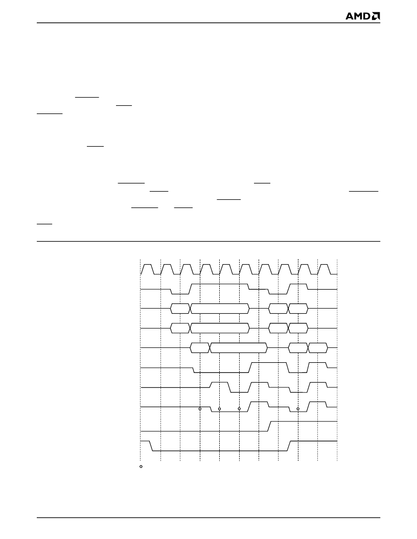
Basic Non-Burst Write Transfer
By default, the Am79C978 controller uses non-burst
cycles in all bus master write operations. All controller
non-burst write accesses are of the PCI command type
Memory Write (type 7). The byte enable signals indi-
Am79C978 controller typically performs more than one
non-burst write transaction within a single bus master-
ship period. FRAME is dropped between consecutive
non-burst write cycles. REQ stays asserted until
FRAME is asserted for the last transaction. The
Am79C978 controller supports zero wait state write cy-
cles except with descriptor write transfers. (See the
section
Descriptor DMA Transfers
for the only excep-
tion.) It asserts IRDY immediately after the address
phase.
Figure 16 shows two non-burst write transactions. The
first transaction has two wait states. The target inserts
one wait state by asserting DEVSEL one clock late and
another wait state by also asserting TRDY one clock
late. The second transaction shows a zero wait state
write cycle. The target asserts DEVSEL and TRDY in
the same cycle as the Am79C978 controller asserts
IRDY.
Basic Burst Write Transfer
The Am79C978 controller supports burst mode for all
bus master write operations. The burst mode must be
enabled by setting BWRITE (BCR18, bit 5). To allow
burst transfers in descriptor write operations, the
Am79C978 controller must also be programmed to use
SWSTYLE 3 (BCR20, bits 7-0). All controller burst
write transfers are of the PCI command type Memory
Write (type 7). AD[1:0] will both be 0 during the address
phase indicating a linear burst order. The byte enable
signals indicate the byte lanes that have valid data.
The Am79C978 controller will always perform a single
burst write transaction per bus mastership period,
where transaction is defined as one address phase and
one or multiple data phases. The Am79C978 controller
supports zero wait state write cycles except with the
case of descriptor write transfers. (See the section
De-
scriptor DMA Transfers
for the only exception.) The de-
vice asserts IRDY immediately after the address phase
and at the same time starts sampling DEVSEL.
FRAME is deasserted when the next to last data phase
is completed.
Figure 16.
Non-Burst Write Transfer
Figure 17 shows a typical burst write access. The
Am79C978 controller arbitrates for the bus, is granted
access, and writes four 32-bit words (DWords) to the
system memory and then releases the bus. In this ex-
FRAME
CLK
AD
IRDY
TRDY
C/
BE
DEVSEL
REQ
GNT
PAR
DEVSEL
is sampled
ADDR
0111
PAR
1
2
3
4
5
6
7
8
10
9
DATA
ADDR
DATA
PAR
PAR
PAR
BE
0111
BE
22206B-19
相關PDF資料 |
PDF描述 |
|---|---|
| AM79C981 | Integrated Multiport Repeater Plus⑩ (IMR+⑩) |
| AM79C981JC | Integrated Multiport Repeater Plus⑩ (IMR+⑩) |
| AM79C982 | basic Integrated Multiport Repeater (bIMR) |
| AM79C982-4JC | basic Integrated Multiport Repeater (bIMR) |
| AM79C982-8JC | basic Integrated Multiport Repeater (bIMR) |
相關代理商/技術參數(shù) |
參數(shù)描述 |
|---|---|
| AM79C978A | 制造商:AMD 制造商全稱:Advanced Micro Devices 功能描述:Single-Chip 1/10 Mbps PCI Home Networking Controller |
| AM79C978AKC\\W | 制造商:Advanced Micro Devices 功能描述: |
| AM79C978AKC\W | 制造商:Advanced Micro Devices 功能描述: |
| AM79C978AKCW | 制造商:AMD 制造商全稱:Advanced Micro Devices 功能描述:Single-Chip 1/10 Mbps PCI Home Networking Controller |
發(fā)布緊急采購,3分鐘左右您將得到回復。