- 您現(xiàn)在的位置:買賣IC網(wǎng) > PDF目錄298814 > ADE7753ARSZRL (ANALOG DEVICES INC) SPECIALTY ANALOG CIRCUIT, PDSO20 PDF資料下載
參數(shù)資料
| 型號(hào): | ADE7753ARSZRL |
| 廠商: | ANALOG DEVICES INC |
| 元件分類: | 模擬信號(hào)調(diào)理 |
| 英文描述: | SPECIALTY ANALOG CIRCUIT, PDSO20 |
| 封裝: | ROHS COMPLIANT, MO-150AE, SSOP-20 |
| 文件頁(yè)數(shù): | 25/60頁(yè) |
| 文件大小: | 938K |
| 代理商: | ADE7753ARSZRL |
第1頁(yè)第2頁(yè)第3頁(yè)第4頁(yè)第5頁(yè)第6頁(yè)第7頁(yè)第8頁(yè)第9頁(yè)第10頁(yè)第11頁(yè)第12頁(yè)第13頁(yè)第14頁(yè)第15頁(yè)第16頁(yè)第17頁(yè)第18頁(yè)第19頁(yè)第20頁(yè)第21頁(yè)第22頁(yè)第23頁(yè)第24頁(yè)當(dāng)前第25頁(yè)第26頁(yè)第27頁(yè)第28頁(yè)第29頁(yè)第30頁(yè)第31頁(yè)第32頁(yè)第33頁(yè)第34頁(yè)第35頁(yè)第36頁(yè)第37頁(yè)第38頁(yè)第39頁(yè)第40頁(yè)第41頁(yè)第42頁(yè)第43頁(yè)第44頁(yè)第45頁(yè)第46頁(yè)第47頁(yè)第48頁(yè)第49頁(yè)第50頁(yè)第51頁(yè)第52頁(yè)第53頁(yè)第54頁(yè)第55頁(yè)第56頁(yè)第57頁(yè)第58頁(yè)第59頁(yè)第60頁(yè)
ADE7753
Rev. C | Page 31 of 60
0xFFFF,FFFF,FFFF before it overflows. The integration time
under these conditions with WDIV = 0 is calculated as follows:
Time =
xCCCCD
0
FFFF
FFFF,
xFFFF,
0
× 1.12 μs = 375.8 s = 6.26 min(15)
When WDIV is set to a value different from 0, the integration
time varies, as shown in Equation 16.
WDIV
Time
WDIV
×
=
=0
(16)
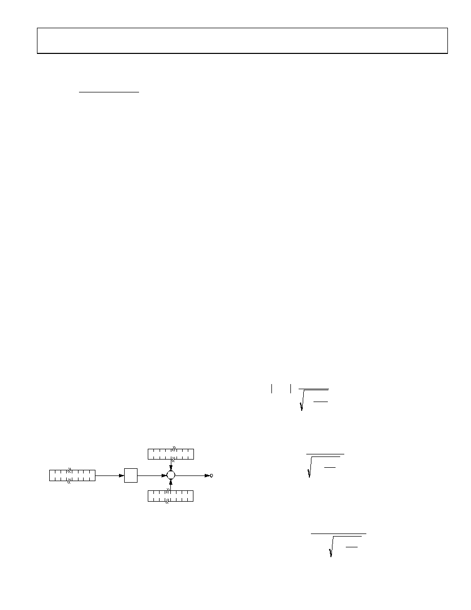
POWER OFFSET CALIBRATION
The ADE7753 also incorporates an active power offset register
(APOS[15:0]). This is a signed twos complement 16-bit register
that can be used to remove offsets in the active power calculation—
see Figure 65. An offset could exist in the power calculation due
to crosstalk between channels on the PCB or in the IC itself.
The offset calibration allows the contents of the active power
register to be maintained at 0 when no power is being consumed.
The 256 LSBs (APOS = 0x0100) written to the active power
offset register are equivalent to 1 LSB in the waveform sample
register. Assuming the average value, output from LPF2 is
0xCCCCD (838,861d) when inputs on Channels 1 and 2 are
both at full scale. At 60 dB down on Channel 1 (1/1000 of the
Channel 1 full-scale input), the average word value output from
LPF2 is 838.861 (838,861/1,000). One LSB in the LPF2 output
has a measurement error of 1/838.861 × 100% = 0.119% of the
average value. The active power offset register has a resolution
equal to 1/256 LSB of the waveform register, therefore the power
offset correction resolution is 0.00047%/LSB (0.119%/256) at –60 dB.
ENERGY-TO-FREQUENCY CONVERSION
ADE7753 also provides energy-to-frequency conversion for
calibration purposes. After initial calibration at manufacturing,
the manufacturer or end customer often verify the energy meter
calibration. One convenient way to verify the meter calibration
is for the manufacturer to provide an output frequency, which is
proportional to the energy or active power under steady load
conditions. This output frequency can provide a simple, single-
wire, optically isolated interface to external calibration
equipment. Figure 67 illustrates the energy-to-frequency
conversion in the ADE7753.
CFNUM[11:0]
CF
11
0
CFDEN[11:0]
11
0
AENERGY[48:0]
48
0
02875-0-066
%
DFC
Figure 67. ADE7753 Energy-to-Frequency Conversion
A digital-to-frequency converter (DFC) is used to generate the
CF pulsed output. The DFC generates a pulse each time 1 LSB
in the active energy register is accumulated. An output pulse is
generated when (CFDEN + 1)/(CFNUM + 1) number of pulses
are generated at the DFC output. Under steady load conditions,
the output frequency is proportional to the active power.
The maximum output frequency, with ac input signals at full scale
and CFNUM = 0x00 and CFDEN = 0x00, is approximately 23 kHz.
The ADE7753 incorporates two registers, CFNUM[11:0] and
CFDEN[11:0], to set the CF frequency. These are unsigned
12-bit registers, which can be used to adjust the CF frequency to
a wide range of values. These frequency-scaling registers are
12-bit registers, which can scale the output frequency by 1/212 to
1 with a step of 1/212.
If the value 0 is written to any of these registers, the value 1
would be applied to the register. The ratio (CFNUM + 1)/
(CFDEN + 1) should be smaller than 1 to ensure proper
operation. If the ratio of the registers (CFNUM + 1)/(CFDEN + 1)
is greater than 1, the register values would be adjusted to a ratio
(CFNUM + 1)/(CFDEN + 1) of 1. For example, if the output
frequency is 1.562 kHz while the contents of CFDEN are 0
(0x000), then the output frequency can be set to 6.1 Hz by
writing 0xFF to the CFDEN register.
When CFNUM and CFDEN are both set to one, the CF pulse
width is fixed at 16 CLKIN/4 clock cycles, approximately 18 μs
with a CLKIN of 3.579545 MHz. If the CF pulse output is
longer than 180 ms for an active energy frequency of less than
5.56 Hz, the pulse width is fixed at 90 ms. Otherwise, the pulse
width is 50% of the duty cycle.
The output frequency has a slight ripple at a frequency equal to
twice the line frequency. This is due to imperfect filtering of the
instantaneous power signal to generate the active power signal—
see the Active Power Calculation section. Equation 9 from the
Active Power Calculation section gives an expression for the
instantaneous power signal. This is filtered by LPF2, which has
a magnitude response given by Equation 17.
2
9
.
8
1
)
(
2
f
H
+
=
(17)
The active power signal (output of LPF2) can be rewritten as
p(t) = VI
+
2
9
.
8
1
L
2f
VI
× cos(4πfLt)
(18)
where fL is the line frequency, for example, 60 Hz.
From Equation 13,
E(t) = VIt
+
π
2
9
.
8
1
4
L
2f
f
VI
× sin(4πfLt)
(19)
相關(guān)PDF資料 |
PDF描述 |
|---|---|
| ADEX-R10+ | 10 MHz - 1000 MHz RF/MICROWAVE DOUBLE BALANCED MIXER, 8.3 dB CONVERSION LOSS-MAX |
| ADF08S | SLIDE DIP SWITCH-8SWITCHES, SPST, LATCHED,SURFACE MOUNT-STRAIGHT |
| ADF09A-KG-TAXB3-R | 9 CONTACT(S), MALE, D SUBMINIATURE CONNECTOR, SOLDER |
| ADF7011BRUZ-RL7 | SPECIALTY TELECOM CIRCUIT, PDSO24 |
| ADF7011BRUZ-RL | SPECIALTY TELECOM CIRCUIT, PDSO24 |
相關(guān)代理商/技術(shù)參數(shù) |
參數(shù)描述 |
|---|---|
| ADE7753-ARSZRL | 制造商:Analog Devices 功能描述: |
| ADE7753XRS | 制造商:Analog Devices 功能描述: |
| ADE7754 | 制造商:AD 制造商全稱:Analog Devices 功能描述:Poly-phase Multi-Function Energy Metering IC with Serial Port |
| ADE7754AR | 制造商:Analog Devices 功能描述:Energy Measurement 24-Pin SOIC W 制造商:Rochester Electronics LLC 功能描述:THREE PHASE ENERGY METER IC W/WATT & VA - Bulk 制造商:Analog Devices 功能描述:IC ENERGY METER |
| ADE7754ARRL | 制造商:Analog Devices 功能描述:Energy Measurement 24-Pin SOIC W T/R 制造商:Rochester Electronics LLC 功能描述:THREE PHASE ENERGY METER IC W/WATT & VA - Bulk |
發(fā)布緊急采購(gòu),3分鐘左右您將得到回復(fù)。