- 您現(xiàn)在的位置:買賣IC網(wǎng) > PDF目錄298814 > ADE7753ARSZRL (ANALOG DEVICES INC) SPECIALTY ANALOG CIRCUIT, PDSO20 PDF資料下載
參數(shù)資料
| 型號: | ADE7753ARSZRL |
| 廠商: | ANALOG DEVICES INC |
| 元件分類: | 模擬信號調(diào)理 |
| 英文描述: | SPECIALTY ANALOG CIRCUIT, PDSO20 |
| 封裝: | ROHS COMPLIANT, MO-150AE, SSOP-20 |
| 文件頁數(shù): | 24/60頁 |
| 文件大小: | 938K |
| 代理商: | ADE7753ARSZRL |
第1頁第2頁第3頁第4頁第5頁第6頁第7頁第8頁第9頁第10頁第11頁第12頁第13頁第14頁第15頁第16頁第17頁第18頁第19頁第20頁第21頁第22頁第23頁當前第24頁第25頁第26頁第27頁第28頁第29頁第30頁第31頁第32頁第33頁第34頁第35頁第36頁第37頁第38頁第39頁第40頁第41頁第42頁第43頁第44頁第45頁第46頁第47頁第48頁第49頁第50頁第51頁第52頁第53頁第54頁第55頁第56頁第57頁第58頁第59頁第60頁
ADE7753
Rev. C | Page 30 of 60
FOR WAVEFORM
ACCUMULATIOIN
1
24
LPF2
V
I
0x19999
0x19999A
0x000000
INSTANTANEOUS
POWER SIGNAL – p(t)
FOR WAVEF0RM
SAMPLING
32
0xCCCCD
CURRENT SIGNAL – i(t)
HPF
VOLTAGE SIGNAL– v(t)
MULTIPLIER
+
APOS [15:0]
26
sgn
25
2-6 2-7 2-8
02875-0-064
WGAIN[11:0]
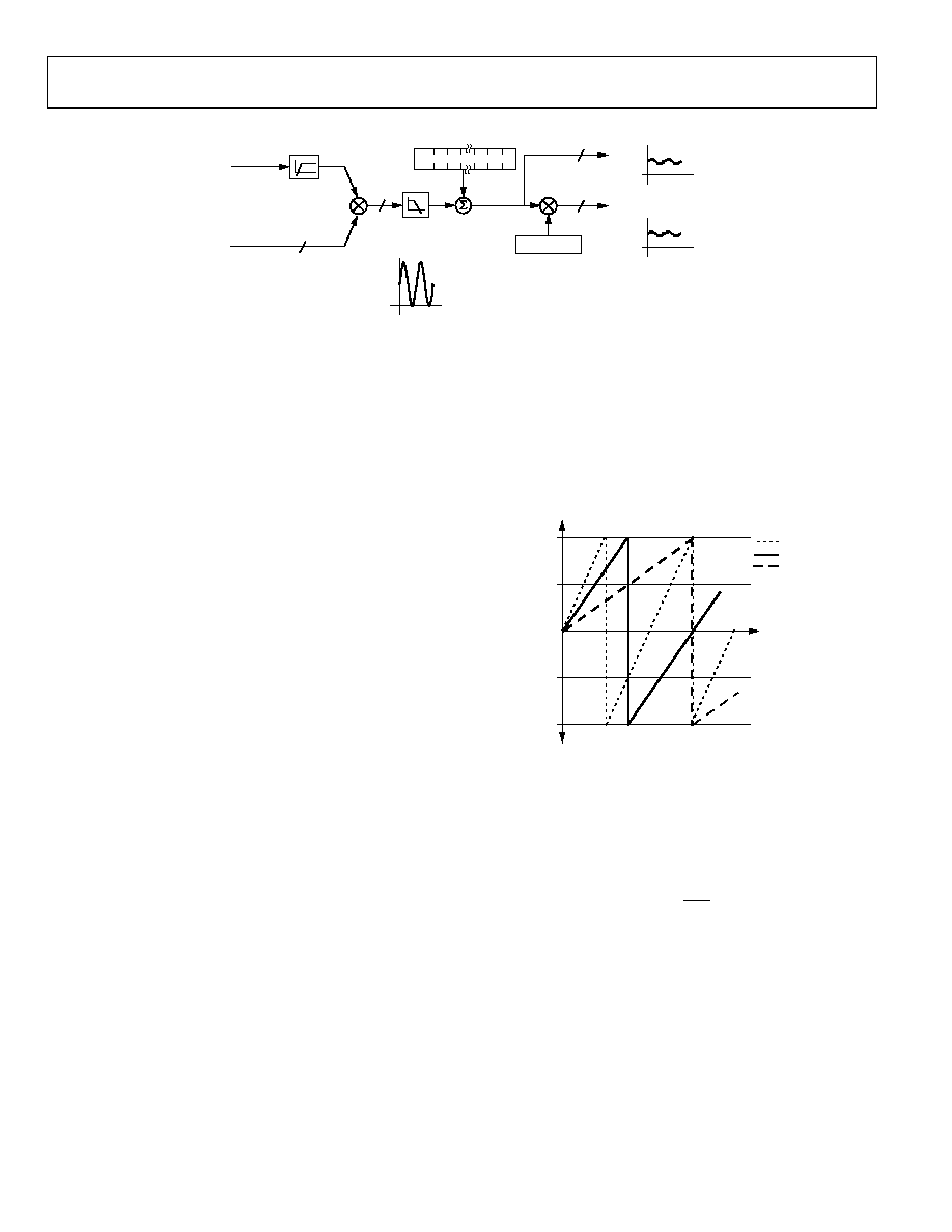
Figure 65. Active Power Signal Processing
The ADE7753 achieves the integration of the active power signal by
continuously accumulating the active power signal in an internal
nonreadable 49-bit energy register. The active energy register
(AENERGY[23:0]) represents the upper 24 bits of this internal
register. This discrete time accumulation or summation is
equivalent to integration in continuous time. Equation 14
expresses the relationship.
×
=
∑
∫
∞
=
→
1
0
)
(
)
(
n
t
T
nT
p
Lim
dt
t
p
E
(14)
where:
n
is the discrete time sample number.
T
is the sample period.
The discrete time sample period (T) for the accumulation
register in the ADE7753 is 1.1μs (4/CLKIN). As well as
calculating the energy, this integration removes any sinusoidal
components that might be in the active power signal. Figure 65
shows this discrete time integration or accumulation. The active
power signal in the waveform register is continuously added to
the internal active energy register. This addition is a signed
addition; therefore negative energy is subtracted from the active
energy contents. The exception to this is when POAM is
selected in the MODE[15:0] register. In this case, only positive
energy contributes to the active energy accumulation—see the
Positive-Only Accumulation Mode section.
The output of the multiplier is divided by WDIV. If the value in
the WDIV register is equal to 0, then the internal active energy
register is divided by 1. WDIV is an 8-bit unsigned register.
After dividing by WDIV, the active energy is accumulated in a
49-bit internal energy accumulation register. The upper 24 bits
of this register are accessible through a read to the active energy
register (AENERGY[23:0]). A read to the RAENERGY register
returns the content of the AENERGY register and the upper 24
bits of the internal register are cleared. As shown in Figure 65, the
active power signal is accumulated in an internal 49-bit signed
register. The active power signal can be read from the waveform
register by setting MODE[14:13] = 0,0 and setting the WSMP
bit (Bit 3) in the interrupt enable register to 1. Like the Channel 1
and Channel 2 waveform sampling modes, the waveform date is
available at sample rates of 27.9 kSPS, 14 kSPS, 7 kSPS, or
3.5 kSPS—see Figure 52.
Figure 66 shows this energy accumulation for full-scale signals
(sinusoidal) on the analog inputs. The three curves displayed
illustrate the minimum period of time it takes the energy register
to roll over when the active power gain register contents are
0x7FF, 0x000, and 0x800. The watt gain register is used to carry
out power calibration in the ADE7753. As shown, the fastest
integration time occurs when the watt gain register is set to
maximum full scale, i.e., 0x7FF.
0x00,0000
0x7F,FFFF
0x3F,FFFF
0x40,0000
0x80,0000
AENERGY [23:0]
6.2
48
12.5
TIME (minutes)
WGAIN = 0x7FF
WGAIN = 0x000
WGAIN = 0x800
02875-0-065
Figure 66. Energy Register Rollover Time for Full-Scale Power
(Minimum and Maximum Power Gain)
Note that the energy register contents rolls over to full-scale
negative (0x800000) and continues to increase in value when
the power or energy flow is positive—see Figure 66. Conversely,
if the power is negative, the energy register underflows to full-
scale positive (0x7FFFFF) and continues to decrease in value.
By using the interrupt enable register, the ADE7753 can be
configured to issue an interrupt (IRQ) when the active energy
register is greater than half-full (positive or negative) or when
an overflow or underflow occurs.
Integration Time under Steady Load
As mentioned in the last section, the discrete time sample
period (T) for the accumulation register is 1.1 μs (4/CLKIN).
With full-scale sinusoidal signals on the analog inputs and the
WGAIN register set to 0x000, the average word value from each
LPF2 is 0xCCCCD—see Figure 61. The maximum positive
value that can be stored in the internal 49-bit register is 248 or
相關(guān)PDF資料 |
PDF描述 |
|---|---|
| ADEX-R10+ | 10 MHz - 1000 MHz RF/MICROWAVE DOUBLE BALANCED MIXER, 8.3 dB CONVERSION LOSS-MAX |
| ADF08S | SLIDE DIP SWITCH-8SWITCHES, SPST, LATCHED,SURFACE MOUNT-STRAIGHT |
| ADF09A-KG-TAXB3-R | 9 CONTACT(S), MALE, D SUBMINIATURE CONNECTOR, SOLDER |
| ADF7011BRUZ-RL7 | SPECIALTY TELECOM CIRCUIT, PDSO24 |
| ADF7011BRUZ-RL | SPECIALTY TELECOM CIRCUIT, PDSO24 |
相關(guān)代理商/技術(shù)參數(shù) |
參數(shù)描述 |
|---|---|
| ADE7753-ARSZRL | 制造商:Analog Devices 功能描述: |
| ADE7753XRS | 制造商:Analog Devices 功能描述: |
| ADE7754 | 制造商:AD 制造商全稱:Analog Devices 功能描述:Poly-phase Multi-Function Energy Metering IC with Serial Port |
| ADE7754AR | 制造商:Analog Devices 功能描述:Energy Measurement 24-Pin SOIC W 制造商:Rochester Electronics LLC 功能描述:THREE PHASE ENERGY METER IC W/WATT & VA - Bulk 制造商:Analog Devices 功能描述:IC ENERGY METER |
| ADE7754ARRL | 制造商:Analog Devices 功能描述:Energy Measurement 24-Pin SOIC W T/R 制造商:Rochester Electronics LLC 功能描述:THREE PHASE ENERGY METER IC W/WATT & VA - Bulk |
發(fā)布緊急采購,3分鐘左右您將得到回復。