- 您現(xiàn)在的位置:買賣IC網(wǎng) > PDF目錄375142 > A48P4616 (AMIC Technology Corporation) CAP 330PF 50V CERAMIC MONO 5% PDF資料下載
參數(shù)資料
| 型號(hào): | A48P4616 |
| 廠商: | AMIC Technology Corporation |
| 英文描述: | CAP 330PF 50V CERAMIC MONO 5% |
| 中文描述: | 16米x 16位DDR內(nèi)存 |
| 文件頁(yè)數(shù): | 50/71頁(yè) |
| 文件大小: | 2068K |
| 代理商: | A48P4616 |
第1頁(yè)第2頁(yè)第3頁(yè)第4頁(yè)第5頁(yè)第6頁(yè)第7頁(yè)第8頁(yè)第9頁(yè)第10頁(yè)第11頁(yè)第12頁(yè)第13頁(yè)第14頁(yè)第15頁(yè)第16頁(yè)第17頁(yè)第18頁(yè)第19頁(yè)第20頁(yè)第21頁(yè)第22頁(yè)第23頁(yè)第24頁(yè)第25頁(yè)第26頁(yè)第27頁(yè)第28頁(yè)第29頁(yè)第30頁(yè)第31頁(yè)第32頁(yè)第33頁(yè)第34頁(yè)第35頁(yè)第36頁(yè)第37頁(yè)第38頁(yè)第39頁(yè)第40頁(yè)第41頁(yè)第42頁(yè)第43頁(yè)第44頁(yè)第45頁(yè)第46頁(yè)第47頁(yè)第48頁(yè)第49頁(yè)當(dāng)前第50頁(yè)第51頁(yè)第52頁(yè)第53頁(yè)第54頁(yè)第55頁(yè)第56頁(yè)第57頁(yè)第58頁(yè)第59頁(yè)第60頁(yè)第61頁(yè)第62頁(yè)第63頁(yè)第64頁(yè)第65頁(yè)第66頁(yè)第67頁(yè)第68頁(yè)第69頁(yè)第70頁(yè)第71頁(yè)
A48P4616
Preliminary (September, 2005, Version 0.0)
49
AMIC Technology, Corp.
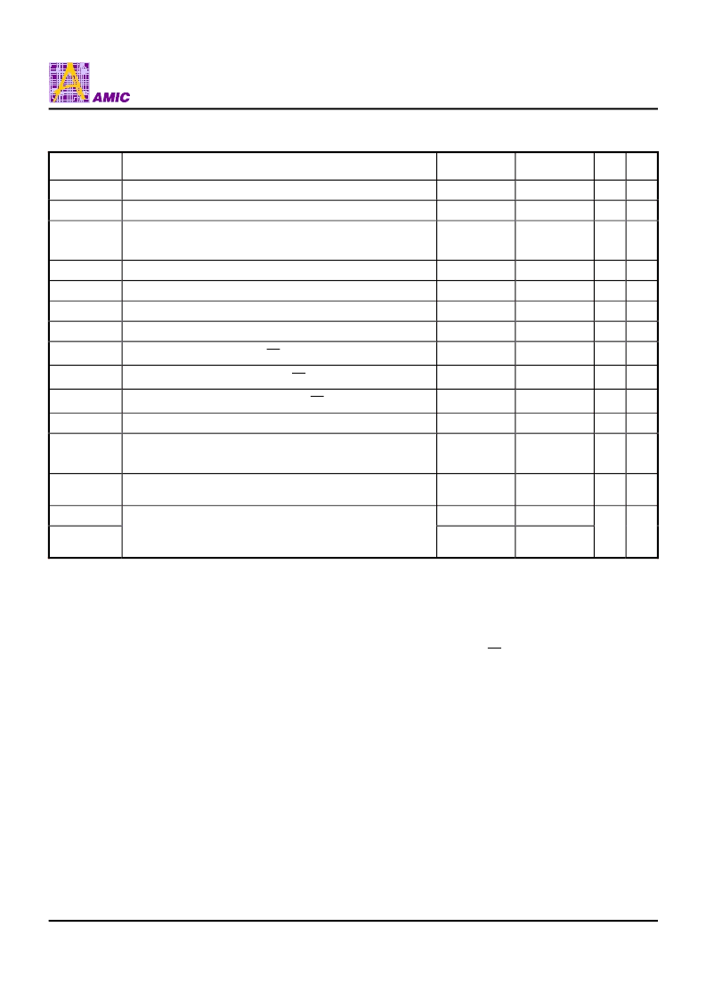
DC Electrical Characteristics and Operating Conditions
(0°C
£
T
A
£
70
×
C; V
DDQ
= 2.5V
±
0.2V, V
DD
=
+
2.5V
±
0.2V, see AC Characteristics)
Symbol
Parameter
Min
Max
Unit Note
V
DD
Supply Voltage
2.3
2.7
V
1
V
DDQ
I/O Supply Voltage
2.3
2.7
V
1
V
SS
, V
SSQ
Supply Voltage
I/O Supply Voltage
0
0
V
V
REF
I/O Reference Voltage
0.49 x V
DDQ
0.51 x V
DDQ
V
1.2
V
TT
I/O Termination Voltage (System)
V
REF
+ 0.04
V
REF
+ 0.04
V
1.3
V
IH (DC)
Input High (Logic 1) Voltage
V
REF
+ 0.15
V
DDQ
+ 0.3
V
1
V
IL (DC)
Input Low (logic 0) Voltage
- 0.3
V
REF
- 0.15
V
1
V
IN (DC)
Input Voltage Level, CK and
CK
Inputs
- 0.3
V
DDQ
+ 0.3
V
1
V
ID (DC)
Input Differential Voltage, CK and
CK
Inputs
0.30
V
DDQ
+ 0.6
V
1.4
V
IX (DC)
Input Crossing Point Voltage, CK and
CK
Inputs
0.30
V
DDQ
+ 0.6
V
1.4
VI
Ratio
V-I Matching Pulup Current to Puldown Current Ratio
0.71
1.4
5
I
I
Input Leakage Current
Any Input 0V
≤
V
OUT
≤
V
DD
; (All other pins not under test = 0V)
Output Leakage Current
(DQs are disabled; 0V
≤
V
OUT
≤
V
DDQ
Output Current: Nominal Strength Driver
High current (V
OUT
= V
DDQ
-0.373V, min V
REF
, min V
TT
)
Low current (V
OUT
= 0.373V, max V
REF
, max V
TT
)
- 5
5
μ
A
1
I
OZ
- 5
5
μ
A
1
I
OH
- 16.8
I
OL
16.8
μ
A
1
Notes:
1. Inputs are not recognized as valid until V
REF
stabilizes.
2. V
REF
is expected to be equal to 0.5 V
DDQ
of the transmitting device, and to track variations in the DC level of the same. Peak-
to-peak noise on V
REF
may not exceed ± 2% of the DC value.
3. V
TT
is not applied directly to the device. V
TT
is a system supply for signal termination resistors, is expected to be set equal to
V
REF
, and must track variations in the DC level of V
REF
.
4. V
ID
is the magnitude of the difference between the input level on CK and the input level on
CK
.
5. The ratio of the pullup current to the pulldown current is specified for the same temperature and voltage, over the entire
temperature and voltage range, for device drain to source voltages for 0.25 volts to 1.0 volts. For a given output, it represents
the maximum difference between pullup and pulldown drivers due to process variation.
相關(guān)PDF資料 |
PDF描述 |
|---|---|
| A49FL004TX-33F | 4 Mbit CMOS 3.3Volt-only Firmware Hub/LPC Flash Memory |
| A49FL004 | 4 Mbit CMOS 3.3Volt-only Firmware Hub/LPC Flash Memory |
| A49FL004TL-33 | 4 Mbit CMOS 3.3Volt-only Firmware Hub/LPC Flash Memory |
| A49FL004TL-33F | 4 Mbit CMOS 3.3Volt-only Firmware Hub/LPC Flash Memory |
| A49FL004TX-33 | 4 Mbit CMOS 3.3Volt-only Firmware Hub/LPC Flash Memory |
相關(guān)代理商/技術(shù)參數(shù) |
參數(shù)描述 |
|---|---|
| A48P48 | 制造商:Pentair Technical Products / Hoffman 功能描述:Panel 44.00x44.00 fits 48.00x4 White, fits 48x48, Steel |
| A-48P48 | 制造商:Pentair Technical Products / Hoffman 功能描述:Panel 44.00x44.00 fits 48.00x4 |
| A48P48G | 制造商:Pentair Technical Products / Hoffman 功能描述:Panel, 44.00X44.00 , fits 48x48, Steel |
| A48PL | 功能描述:ANT TWO-WAY 48MHZ PL CONN RoHS:是 類別:RF/IF 和 RFID >> RF 天線 系列:- 標(biāo)準(zhǔn)包裝:1 系列:* |
| A48R3612HCR | 制造商:Pentair Technical Products / Hoffman 功能描述:Type 3R Enclosure, Hng Cover |
發(fā)布緊急采購(gòu),3分鐘左右您將得到回復(fù)。