- 您現(xiàn)在的位置:買賣IC網(wǎng) > PDF目錄378216 > 82595TX (INTEL CORP) ISA/PCMCIA HIGH INTEGRATION ETHERNET CONTROLLER PDF資料下載
參數(shù)資料
| 型號(hào): | 82595TX |
| 廠商: | INTEL CORP |
| 元件分類: | 微控制器/微處理器 |
| 英文描述: | ISA/PCMCIA HIGH INTEGRATION ETHERNET CONTROLLER |
| 中文描述: | 2 CHANNEL(S), 10M bps, LOCAL AREA NETWORK CONTROLLER, PQFP144 |
| 封裝: | TQFP-144 |
| 文件頁數(shù): | 35/54頁 |
| 文件大?。?/td> | 643K |
| 代理商: | 82595TX |
第1頁第2頁第3頁第4頁第5頁第6頁第7頁第8頁第9頁第10頁第11頁第12頁第13頁第14頁第15頁第16頁第17頁第18頁第19頁第20頁第21頁第22頁第23頁第24頁第25頁第26頁第27頁第28頁第29頁第30頁第31頁第32頁第33頁第34頁當(dāng)前第35頁第36頁第37頁第38頁第39頁第40頁第41頁第42頁第43頁第44頁第45頁第46頁第47頁第48頁第49頁第50頁第51頁第52頁第53頁第54頁
82595FX
11.0
ELECTRICAL SPECIFICATIONS
AND TIMINGS
11.1 Absolute Maximum Ratings
Case Temperature under Bias ààààààà0
§
C to
a
85
§
C
Storage Temperature àààààààààà
b
65
§
C to
a
140
§
C
All Output and Supply Voltages ààààà
b
0.5V to
a
7V
All Input Voltages ààààààààààààà
b
1.0V to
a
6.0V
(1)
Further information on the quality and reliability of
the 82595FX may be found in the Components
Quality and Reliability Handbook, Order Number
210997.
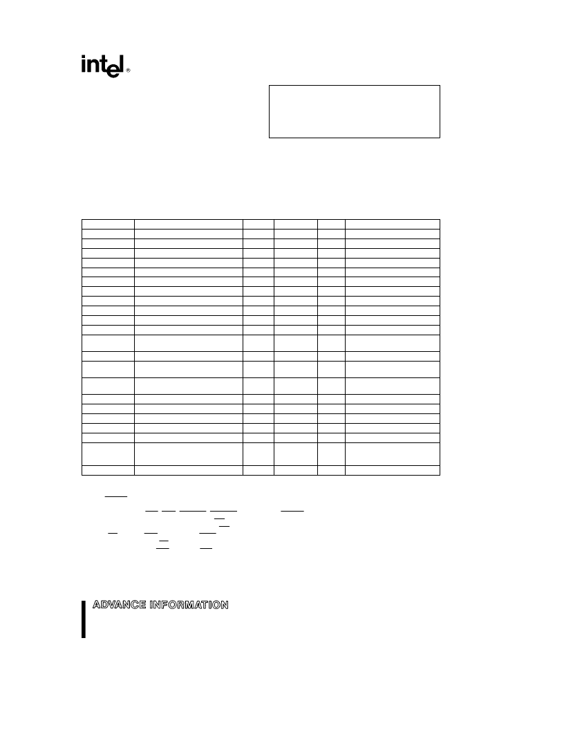
Table 11-1. DC Characteristics
(T
C
e
0
§
C to
a
85
§
C, V
CC
e
5V
g
5%)
Symbol
Parameter
V
IL
Input LOW Voltage (TTL)
V
IH
Input HIGH Voltage (TTL)
V
IH(JUMPR)
Input HIGH Voltage (Jumpers)
V
OL1(2)
Output LOW Voltage
V
OL2(3)
Output LOW Voltage
V
OL4(4)
Output LOW Voltage
V
OH
Output HIGH Voltage
V
OL
(LED)
(5)
Output Low Voltage
V
OH
(LED)
Output High Voltage
I
LP(6)
Leakage Current
R
DIFF(7)
Input Differential-Resistance
V
IDF
(TPE)
(8)
Input Differential Accept
Input Differential Reject
R
S
(TPE)
(9)
Output Source Resistance
V
IDF
(AUI)
(10)
Input Differential Accept
Input Differential Reject
V
ICM
(AUI)
(11)
AC Input Common Mode
NOTICE: This data sheet contains information on
products in the sampling and initial production phases
of development. The specifications are subject to
change without notice. Verify with your local Intel
Sales office that you have the latest data sheet be-
fore finalizing a design.
*
WARNING: Stressing the device beyond the ‘‘Absolute
Maximum Ratings’’ may cause permanent damage.
These are stress ratings only. Operation beyond the
‘‘Operating Conditions’’ is not recommended and ex-
tended exposure beyond the ‘‘Operating Conditions’’
may affect device reliability.
Min
b
0.3
2.0
3.0
Max
a
0.8
Units
V
V
V
V
V
V
V
V
V
m
A
K
X
V
P
V
P
X
V
P
V
P
V
P
V
P
V
mA
mV
mV
mA
m
A
mA
mA
pF
Test Conditions
V
CC
a
0.3
V
CC
a
0.3
0.45
0.45
0.45
I
OL
e
17 mA
I
OL
e
12 mA
I
OL
e
2 mA
I
OH
e b
1 mA
I
OL
e
10 mA
I
OH
e b
500
m
A
0
s
V
I
s
V
CC
DC
5 MHz
s
f
s
10 MHz
2.4
0.45
3.9
g
10
10
g
0.5
g
3.1
g
0.3
13
5
l
I
LOAD
l
e
25 mA
g
0.3
g
1.5
g
0.16
g
0.5
g
0.1
g
1.2
g
150
b
100
40
90
400
2
35
10
f
s
40 KHz
40 KHz
s
f
s
10 MHz
V
ODF
(AUI)
I
OSC
(AUI)
VU (AUI)
V
ODI
(AUI)
(12)
I
CC
I
CCHWPD
I
CCSWPD
I
CCSLEEP
C
IN(13)
Output Differential Voltage
AUI Output Short Circuit Current
Output Differential Undershoot
Differential Idle Voltage
Power Supply Current
Hardware Power Down
Software Power Down
Sleep Mode
Input Capacitance
g
0.45
Short Circuit to V
CC
or GND
@
f
e
1 MHz
NOTES:
1. The voltage level for RCV and CLSN pairs are
b
0.75V to
a
8.5V.
2. SDx, IOCS16.
3. IOCHRDY, IRQx.
4. LDATAx, LADDRx, LOE, LWE, BOOTCS, SRAMCS, EEPROMCS, SMOUT, TSTCLK, TDO, J1, J2.
5. LILED, ACTLED, POLED and TPEDBNCDAUI.
6. Pins: ACTLED, LILED, POLED, TPEDBNCDAUI.
7. RD to RD, RCV to RCV and CLSN to CLSN.
8. TPE input pins: RD and RD.
9. TPE output pins: TDH, TDH, TDL and TDL, R
S
measure V
CC
or V
SS
to pin.
10. AUI input pins: RCV and CLSN pairs.
11. AUI output pins: TPMT pair.
12. Measured 8.0
m
s after last positive transition of data packet.
13. Characterized, not tested.
35
相關(guān)PDF資料 |
PDF描述 |
|---|---|
| 82596DX | HIGH-PERFORMANCE 32-BIT LOCAL AREA NETWORK COPROCESSOR |
| 82596SX | HIGH-PERFORMANCE 32-BIT LOCAL AREA NETWORK COPROCESSOR |
| 82596CA | HIGH-PERFORMANCE 32-BIT LOCAL AREA NETWORK COPROCESSOR |
| 8261SHAKE22 | Alternate Action and Momentary Pushbutton Switches |
| 8261SHAKE223 | Alternate Action and Momentary Pushbutton Switches |
相關(guān)代理商/技術(shù)參數(shù) |
參數(shù)描述 |
|---|---|
| 82596 | 制造商:TE Connectivity 功能描述:STD TERM/SPLICE WALL CHART - Bulk |
| 82596CA | 制造商:INTEL 制造商全稱:Intel Corporation 功能描述:HIGH-PERFORMANCE 32-BIT LOCAL AREA NETWORK COPROCESSOR |
| 82596DX | 制造商:INTEL 制造商全稱:Intel Corporation 功能描述:HIGH-PERFORMANCE 32-BIT LOCAL AREA NETWORK COPROCESSOR |
| 82596SX | 制造商:INTEL 制造商全稱:Intel Corporation 功能描述:HIGH-PERFORMANCE 32-BIT LOCAL AREA NETWORK COPROCESSOR |
| 82598 | 制造商:INTEL 制造商全稱:Intel Corporation 功能描述:10 GbE Controller |
發(fā)布緊急采購(gòu),3分鐘左右您將得到回復(fù)。