- 您現(xiàn)在的位置:買賣IC網(wǎng) > PDF目錄373783 > ZL30109 (Zarlink Semiconductor Inc.) DS1/E1 System Synchronizer with 19.44 MHz Output PDF資料下載
參數(shù)資料
| 型號(hào): | ZL30109 |
| 廠商: | Zarlink Semiconductor Inc. |
| 英文描述: | DS1/E1 System Synchronizer with 19.44 MHz Output |
| 中文描述: | 的DS1/E1系統(tǒng)同步與19.44 MHz輸出 |
| 文件頁(yè)數(shù): | 6/36頁(yè) |
| 文件大?。?/td> | 474K |
| 代理商: | ZL30109 |
第1頁(yè)第2頁(yè)第3頁(yè)第4頁(yè)第5頁(yè)當(dāng)前第6頁(yè)第7頁(yè)第8頁(yè)第9頁(yè)第10頁(yè)第11頁(yè)第12頁(yè)第13頁(yè)第14頁(yè)第15頁(yè)第16頁(yè)第17頁(yè)第18頁(yè)第19頁(yè)第20頁(yè)第21頁(yè)第22頁(yè)第23頁(yè)第24頁(yè)第25頁(yè)第26頁(yè)第27頁(yè)第28頁(yè)第29頁(yè)第30頁(yè)第31頁(yè)第32頁(yè)第33頁(yè)第34頁(yè)第35頁(yè)第36頁(yè)
ZL30109
Data Sheet
6
Zarlink Semiconductor Inc.
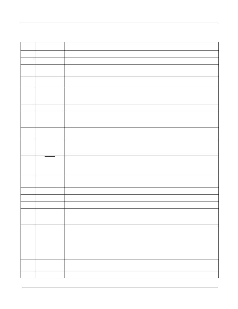
1.0 Pin Description
Pin Description
Pin #
Name
Description
1
GND
Ground.
0 V.
2
V
CORE
LOCK
Positive Supply Voltage.
+1.8 V
DC
nominal.
Lock Indicator (Output).
This output goes to a logic high when the PLL is frequency
locked to the selected input reference.
3
4
HOLDOVER
Holdover (Output).
This output goes to a logic high whenever the PLL goes into
holdover mode.
5
REF_FAIL0
Reference 0 Failure Indicator (Output).
A logic high at this pin indicates that the REF0
reference frequency has exceeded the out-of-range limit set by the OOR_SEL pin or that
it is exhibiting abrupt phase or frequency changes.
6
IC
Internal bonding Connection.
Leave unconnected.
7
REF_FAIL1
Reference 1 Failure Indicator (Output).
A logic high at this pin indicates that the REF1
reference frequency has exceeded the out-of-range limit set by the OOR_SEL pin or that
it is exhibiting abrupt phase or frequency changes.
8
TDO
Test Serial Data Out (Output).
JTAG serial data is output on this pin on the falling edge
of TCK. This pin is held in high impedance state when JTAG scan is not enabled.
9
TMS
Test Mode Select (Input).
JTAG signal that controls the state transitions of the TAP
controller. This pin is internally pulled up to V
DD
. If this pin is not used then it should be
left unconnected.
10
TRST
Test Reset (Input).
Asynchronously initializes the JTAG TAP controller by putting it in
the Test-Logic-Reset state. This pin should be pulsed low on power-up to ensure that
the device is in the normal functional state. This pin is internally pulled up to V
DD
. If
this pin is not used then it should be connected to GND.
11
TCK
Test Clock (Input):
Provides the clock to the JTAG test logic. If this pin is not used then it
should be pulled down to GND.
12
V
CORE
GND
Positive Supply Voltage.
+1.8 V
DC
nominal.
Ground.
0 V.
13
14
AV
CORE
TDI
Positive Analog Supply Voltage.
+1.8 V
DC
nominal.
Test Serial Data In (Input).
JTAG serial test instructions and data are shifted in on this
pin. This pin is internally pulled up to V
DD
. If this pin is not used then it should be left
unconnected.
15
16
HMS
Hitless Mode Switching (Input).
The HMS circuit controls phase accumulation during
the transition from Holdover or Freerun mode to Normal mode on the same reference. A
logic low at this pin will cause the ZL30109 to maintain the delay stored in the TIE
corrector circuit when it transitions from Holdover or Freerun mode to Normal mode. A
logic high on this pin will cause the ZL30109 to measure a new delay for its TIE corrector
circuit thereby minimizing the output phase movement when it transitions from Holdover
or Freerun mode to Normal mode.
17
MODE_SEL0
Mode Select 0 (Input).
This input combined with MODE_SEL1 determines the mode
(Normal, Holdover or Freerun) of operation, see Table 4 on page 17.
18
MODE_SEL1
Mode Select 1 (Input).
See MODE_SEL0 pin description.
相關(guān)PDF資料 |
PDF描述 |
|---|---|
| ZL30109QDG | DS1/E1 System Synchronizer with 19.44 MHz Output |
| ZL30110 | Telecom Rate Conversion DPLL |
| ZL30110LDE | Telecom Rate Conversion DPLL |
| ZL30110LDE1 | Telecom Rate Conversion DPLL |
| ZL30111 | POTS Line Card PLL |
相關(guān)代理商/技術(shù)參數(shù) |
參數(shù)描述 |
|---|---|
| ZL30109_05 | 制造商:ZARLINK 制造商全稱:Zarlink Semiconductor Inc 功能描述:DS1/E1 System Synchronizer with |
| ZL30109QDG | 制造商:Microsemi Corporation 功能描述: |
| ZL30109QDG1 | 制造商:Microsemi Corporation 功能描述:DS1/E1 System Synchronizer 64-Pin TQFP 制造商:Microsemi Corporation 功能描述:DS1/E1 SYS. SYNCH WITH 19.44MHZ 制造商:Microsemi Corporation 功能描述:DS1/E1 SYS SYNCHRONIZER 64TQFP - Trays 制造商:MICROSEMI CONSUMER MEDICAL PRODUCT GROUP 功能描述:IC SYNCHRONIZER DPLL 64TQFP 制造商:Microsemi Corporation 功能描述:IC SYNCHRONIZER DPLL 64TQFP |
| ZL30110 | 制造商:ZARLINK 制造商全稱:Zarlink Semiconductor Inc 功能描述:Telecom Rate Conversion DPLL |
| ZL30110LDE | 制造商:Microsemi Corporation 功能描述: 制造商:Microsemi Corporation 功能描述:PLL FREQ SYNTHESIZER TRIPLE 32QFN - Rail/Tube |
發(fā)布緊急采購(gòu),3分鐘左右您將得到回復(fù)。