- 您現(xiàn)在的位置:買賣IC網(wǎng) > PDF目錄373783 > ZL30100QDG1 (ZARLINK SEMICONDUCTOR INC) T1/E1 System Synchronizer PDF資料下載
參數(shù)資料
| 型號(hào): | ZL30100QDG1 |
| 廠商: | ZARLINK SEMICONDUCTOR INC |
| 元件分類: | 通信及網(wǎng)絡(luò) |
| 英文描述: | T1/E1 System Synchronizer |
| 中文描述: | SPECIALTY TELECOM CIRCUIT, PQFP64 |
| 封裝: | 10 X 10 MM, 1 MM HEIGHT, LEAD FREE, MS-026ACD, TQFP-64 |
| 文件頁(yè)數(shù): | 14/36頁(yè) |
| 文件大小: | 346K |
| 代理商: | ZL30100QDG1 |
第1頁(yè)第2頁(yè)第3頁(yè)第4頁(yè)第5頁(yè)第6頁(yè)第7頁(yè)第8頁(yè)第9頁(yè)第10頁(yè)第11頁(yè)第12頁(yè)第13頁(yè)當(dāng)前第14頁(yè)第15頁(yè)第16頁(yè)第17頁(yè)第18頁(yè)第19頁(yè)第20頁(yè)第21頁(yè)第22頁(yè)第23頁(yè)第24頁(yè)第25頁(yè)第26頁(yè)第27頁(yè)第28頁(yè)第29頁(yè)第30頁(yè)第31頁(yè)第32頁(yè)第33頁(yè)第34頁(yè)第35頁(yè)第36頁(yè)
ZL30100
Data Sheet
14
Zarlink Semiconductor Inc.
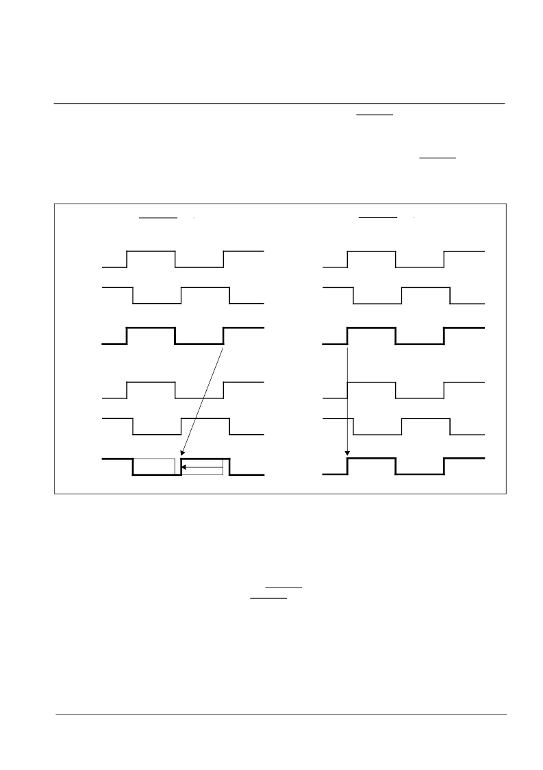
The delay value can be reset by setting the TIE corrector circuit clear pin (TIE_CLR) low for at least 15 ns. This
results in a phase alignment between the input reference signal and the output clocks and frame pulses as shown
in Figure 16 on page 29 and Figure 17 on page 31. The speed of the phase alignment correction is limited to
61
μ
s/s when BW_SEL=0. Convergence is always in the direction of least phase travel. In general the TIE
correction should not be exercised when Holdover mode is entered for short time periods. TIE_CLR can be kept
low continuously. In that case the output clocks will always be aligned with the selected input reference. This is
illustrated in Figure 7.
Figure 7 - Timing Diagram of Hitless Reference Switching
The Hitless Mode Switching (HMS) pin enables phase hitless returns from Freerun and Holdover modes to Normal
mode in a single reference operation. A logic low at the HMS input disables the TIE corrector circuit updating the
delay value thereby forcing the output of the PLL to gradually move back to the original point before it went into
Holdover mode. (see Figure 8). This prevents accumulation of phase in network elements. A logic high (HMS=1)
enables the TIE corrector circuit to update its delay value thereby preventing a large output phase movement after
return to Normal mode. This causes accumulation of phase in network elements. In both cases the PLL’s output
can be aligned with the input reference by setting TIE_CLR low. Regardless of the HMS pin state, reference
switching in the ZL30100 is always hitless unless TIE_CLR is kept low continuously.
locked to REF1
REF0
Output
Clock
TIE_CLR = 1
TIE_CLR = 0
REF1
REF0
Output
Clock
REF1
locked to REF1
REF0
Output
Clock
REF1
REF0
Output
Clock
REF1
locked to REF0
locked to REF0
相關(guān)PDF資料 |
PDF描述 |
|---|---|
| ZL30100 | T1/E1 System Synchronizer |
| ZL30100QDC | T1/E1 System Synchronizer |
| ZL30101QDG1 | T1/E1 Stratum 3 System Synchronizer |
| ZL30101 | T1/E1 Stratum 3 System Synchronizer |
| ZL30101QDC | T1/E1 Stratum 3 System Synchronizer |
相關(guān)代理商/技術(shù)參數(shù) |
參數(shù)描述 |
|---|---|
| ZL30101 | 制造商:ZARLINK 制造商全稱:Zarlink Semiconductor Inc 功能描述:T1/E1 Stratum 3 System Synchronizer |
| ZL30101_06 | 制造商:ZARLINK 制造商全稱:Zarlink Semiconductor Inc 功能描述:T1/E1 Stratum 3 System Synchronizer |
| ZL30101QDC | 制造商:Microsemi Corporation 功能描述: |
| ZL30101QDG1 | 制造商:Microsemi Corporation 功能描述:SYS SYNCHRONIZER 64TQFP - Trays |
| ZL30102 | 制造商:ZARLINK 制造商全稱:Zarlink Semiconductor Inc 功能描述:T1/E1 Stratum 4/4E Redundant System Clock Synchronizer for DS1/E1 and H.110 |
發(fā)布緊急采購(gòu),3分鐘左右您將得到回復(fù)。