- 您現(xiàn)在的位置:買賣IC網(wǎng) > PDF目錄1977 > XRT94L31IB-L (Exar Corporation)IC MAPPER DS3/E3/STS-1 504TBGA PDF資料下載
參數(shù)資料
| 型號: | XRT94L31IB-L |
| 廠商: | Exar Corporation |
| 文件頁數(shù): | 25/133頁 |
| 文件大?。?/td> | 0K |
| 描述: | IC MAPPER DS3/E3/STS-1 504TBGA |
| 標(biāo)準(zhǔn)包裝: | 24 |
| 應(yīng)用: | 網(wǎng)絡(luò)切換 |
| 接口: | 總線 |
| 電源電壓: | 3.14 V ~ 3.47 V |
| 封裝/外殼: | 504-LBGA |
| 供應(yīng)商設(shè)備封裝: | 504-TBGA(35x35) |
| 包裝: | 托盤 |
| 安裝類型: | 表面貼裝 |
第1頁第2頁第3頁第4頁第5頁第6頁第7頁第8頁第9頁第10頁第11頁第12頁第13頁第14頁第15頁第16頁第17頁第18頁第19頁第20頁第21頁第22頁第23頁第24頁當(dāng)前第25頁第26頁第27頁第28頁第29頁第30頁第31頁第32頁第33頁第34頁第35頁第36頁第37頁第38頁第39頁第40頁第41頁第42頁第43頁第44頁第45頁第46頁第47頁第48頁第49頁第50頁第51頁第52頁第53頁第54頁第55頁第56頁第57頁第58頁第59頁第60頁第61頁第62頁第63頁第64頁第65頁第66頁第67頁第68頁第69頁第70頁第71頁第72頁第73頁第74頁第75頁第76頁第77頁第78頁第79頁第80頁第81頁第82頁第83頁第84頁第85頁第86頁第87頁第88頁第89頁第90頁第91頁第92頁第93頁第94頁第95頁第96頁第97頁第98頁第99頁第100頁第101頁第102頁第103頁第104頁第105頁第106頁第107頁第108頁第109頁第110頁第111頁第112頁第113頁第114頁第115頁第116頁第117頁第118頁第119頁第120頁第121頁第122頁第123頁第124頁第125頁第126頁第127頁第128頁第129頁第130頁第131頁第132頁第133頁
XRT94L31
120
3-CHANNEL DS3/E3/STS-1 TO STS-3/STM-1 MAPPER IC
REV. 1.0.1
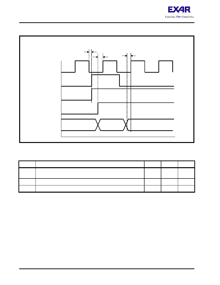
NOTE: The values for t18, t19 and t20 can be found in
1.7
TRANSMIT ORDERWIRE (E1, F1, E2) BYTE OVERHEAD INPUT PORT
The Transmit Order-wire Byte Overhead Input Port provides a dedicated port for the user to insert his/her own
value for the E1, F1 and E2 bytes within the outbound STS-3/STM-1 data-stream. The user should note that
the TxE1F1E2 input pin is sampled (by the Transmit Order-wire Byte Overhead Input Port) upon the rising
edge of TxTOHClk. All of the remaining signals (e.g., TxE1F1E2Enable, TxE1F1E2Frame) are updated upon
the falling edge of TxTOHClk. The timing wave-form and information for the Transmit Order-wire Byte
Overhead Input Port is presented below.
FIGURE 23. ILLUSTRATION OF TIMING WAVE-FORM OF THE TRANSMIT POH OVERHEAD INPUT PORT
TABLE 24: TIMING INFORMATION FOR THE TRANSMIT POH OVERHEAD INPUT PORT
SYMBOL
DESCRIPTION
MIN.
TYP.
MAX.
t18
Falling edge of TxPOHClk to rising edge of TxPOHFrame and TxPOHValid
output delay
-0.3ns
0.2ns
t19
TxPOHIns to rising edge of TxPOHClk set-up time
4ns
t20
TxPOH Data to rising edge of TxPOHClk set-up time
4ns
TxPOH
TxPOHIns
TxPOHClk
TxPOHFrame
TxPOHEnable
t18
t19
t20
相關(guān)PDF資料 |
PDF描述 |
|---|---|
| XRT94L33IB-L | IC MAPPER DS3/E3/STS-1 504TBGA |
| XRT94L43IB-F | IC MAPPER SONET/SDH OC12 516BGA |
| XS1-G02B-FB144-I4 | IC MCU 32BIT 16KB OTP 144FBGA |
| XTR114U/2K5 | IC 4-20MA I-TRANSMITTER 14-SOIC |
| ZXHF5000JB24TC | IC SWITCH QUAD 2X1 24QFN |
相關(guān)代理商/技術(shù)參數(shù) |
參數(shù)描述 |
|---|---|
| XRT94L33 | 制造商:EXAR 制造商全稱:EXAR 功能描述:-CHANNEL DS3/E3/STS-1 TO STS-3/STM-1 MAPPER - SONET REGISTERS |
| XRT94L33_06 | 制造商:EXAR 制造商全稱:EXAR 功能描述:3-CHANNEL DS3/E3/STS-1 TO STS-3/STM-1 MAPPER IC DATA SHEET |
| XRT94L33_07 | 制造商:EXAR 制造商全稱:EXAR 功能描述:3-CHANNEL DS3/E3/STS-1 TO STS-3/STM-1 MAPPER - ATM REGISTERS |
| XRT94L33_1 | 制造商:EXAR 制造商全稱:EXAR 功能描述:3-CHANNEL DS3/E3/STS-1 TO STS-3/STM-1 MAPPER ATM/PPP - HARWARE MANUAL |
| XRT94L33_2 | 制造商:EXAR 制造商全稱:EXAR 功能描述:3-CHANNEL DS3/E3/STS-1 TO STS-3/STM-1 MAPPER - SDH REGISTERS |
發(fā)布緊急采購,3分鐘左右您將得到回復(fù)。