- 您現(xiàn)在的位置:買賣IC網(wǎng) > PDF目錄202172 > V58C2256324SAH-36 (PROMOS TECHNOLOGIES INC) 8M X 32 DDR DRAM, 0.55 ns, PBGA144 PDF資料下載
參數(shù)資料
| 型號: | V58C2256324SAH-36 |
| 廠商: | PROMOS TECHNOLOGIES INC |
| 元件分類: | DRAM |
| 英文描述: | 8M X 32 DDR DRAM, 0.55 ns, PBGA144 |
| 封裝: | ROHS COMPLIANT, BGA-144 |
| 文件頁數(shù): | 32/37頁 |
| 文件大小: | 370K |
| 代理商: | V58C2256324SAH-36 |
第1頁第2頁第3頁第4頁第5頁第6頁第7頁第8頁第9頁第10頁第11頁第12頁第13頁第14頁第15頁第16頁第17頁第18頁第19頁第20頁第21頁第22頁第23頁第24頁第25頁第26頁第27頁第28頁第29頁第30頁第31頁當(dāng)前第32頁第33頁第34頁第35頁第36頁第37頁
4
V58C2256324SA Rev. 1.4 August 2007
ProMOS TECHNOLOGIES
V58C2256324SA
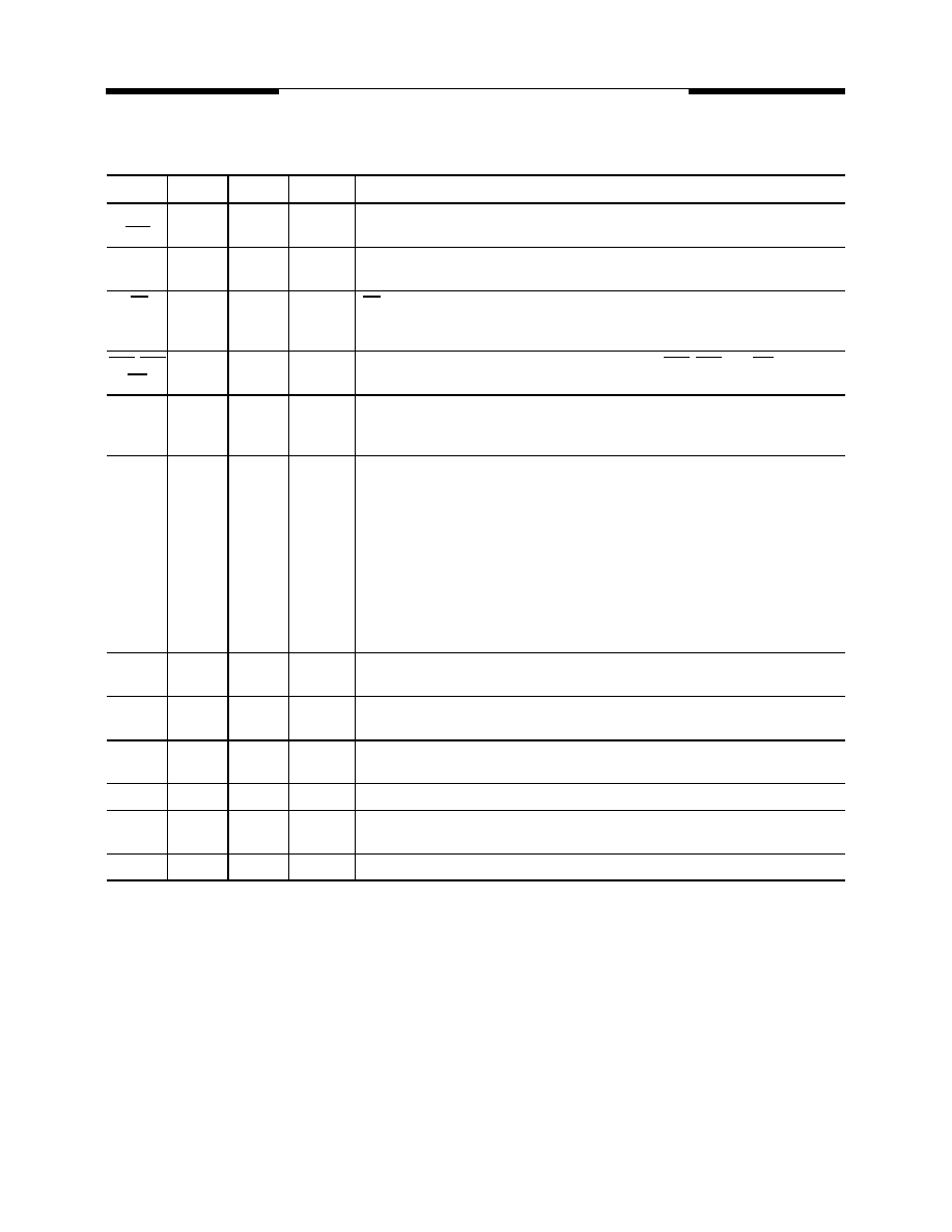
Signal Pin Description
Pin
Type
Signal
Polarity
Function
CLK
Input
Pulse
Positive
Edge
The system clock input. All inputs except DQs and DMs are sampled on the rising edge
of CLK.
CKE
Input
Level
Active High Activates the CLK signal when high and deactivates the CLK signal when low, thereby
initiates either the Power Down mode, Suspend mode, or the Self Refresh mode.
CS
Input
Pulse
Active Low CS enables the command decoder when low and disables the command decoder when
high. When the command decoder is disabled, new commands are ignored but previous
operations continue.
RAS, CAS
WE
Input
Pulse
Active Low When sampled at the positive rising edge of the clock, CAS, RAS, and WE define the
command to be executed by the SDRAM.
DQS
Input/
Output
Pulse
Active High Active on both edges for data input and output.
Center aligned to input data
Edge aligned to output data
A0 - A11
Input
Level
—
During a Bank Activate command cycle, A0-A11 defines the row address (RA0-RA11)
when sampled at the rising clock edge.
During a Read or Write command cycle, A0-A7, A9 defines the column address (CA0-
CA7, CA9) when sampled at the rising clock edge.
In addition to the column address, A8 is used to invoke autoprecharge operation at the
end of the burst read or write cycle. If A8 is high, autoprecharge is selected and BA0, BA1
defines the bank to be precharged. If A8 is low, autoprecharge is disabled.
During a Precharge command cycle, A8(=AP) is used in conjunction with BA0 and BA1
to control which bank(s) to precharge. If A8 is high, all four banks will be precharged
simultaneously regardless of state of BA0 and BA1.
BA0,
BA1
Input
Level
—
Selects which bank is to be active.
DQS0-
DQS3
Input/
Output
Level
—
Data Input/Output are synchronous withboth edges of the DQS. DQS0 for DQ0-DQ7,
DQS1 for DQ8-DQ15, DQS2 for DQ16-DQ23 and DQS3 for DQ24-DQ31.
DM0-DM3
Input
Pulse
Active High In Write mode, DM has a latency of zero and operates as a word mask by allowing input
data to be written if it is low but blocks the write operation if is high.
VDD, VSS
Supply
Power and ground for the input buffers and the core logic.
VDDQ
VSSQ
Supply
—
Isolated power supply and ground for the output buffers to provide improved noise
immunity.
VREF
Input
Level
—
SSTL Reference Voltage for Inputs
相關(guān)PDF資料 |
PDF描述 |
|---|---|
| V58C2256404SBJ5 | 64M X 4 DDR DRAM, 0.65 ns, PBGA60 |
| V58C2256164SBLJ5B | 16M X 16 DDR DRAM, 0.65 ns, PBGA60 |
| V58C2256404SCLS7I | 64M X 4 DDR DRAM, 0.75 ns, PBGA60 |
| V58C2256404SHUT6E | 64M X 4 DDR DRAM, PDSO66 |
| V58C2256804SHLJ5E | 32M X 8 DDR DRAM, PBGA60 |
相關(guān)代理商/技術(shù)參數(shù) |
參數(shù)描述 |
|---|---|
| V58C2256404S | 制造商:MOSEL 制造商全稱:MOSEL 功能描述:HIGH PERFORMANCE 2.5 VOLT 256 Mbit DDR SDRAM |
| V58C2256804S | 制造商:MOSEL 制造商全稱:MOSEL 功能描述:HIGH PERFORMANCE 2.5 VOLT 256 Mbit DDR SDRAM |
| V58C2256804SAT-5 | 制造商:Mosel Vitelic Corporation 功能描述:SDRAM, DDR, 32M x 8, 66 Pin, Plastic, TSSOP |
| V58C265164S | 制造商:MOSEL 制造商全稱:MOSEL 功能描述:64 Mbit DDR SDRAM 2.5 VOLT 4M X 16 |
| V58C265404S | 制造商:MOSEL 制造商全稱:MOSEL 功能描述:HIGH PERFORMANCE 2.5 VOLT 16M X 4 DDR SDRAM 4 BANKS X 4Mbit X 4 |
發(fā)布緊急采購,3分鐘左右您將得到回復(fù)。