- 您現(xiàn)在的位置:買賣IC網(wǎng) > PDF目錄300064 > UPD78011HGK-XXX-8A8 8-BIT, MROM, 10 MHz, MICROCONTROLLER, PQFP64 PDF資料下載
參數(shù)資料
| 型號: | UPD78011HGK-XXX-8A8 |
| 元件分類: | 微控制器/微處理器 |
| 英文描述: | 8-BIT, MROM, 10 MHz, MICROCONTROLLER, PQFP64 |
| 封裝: | 12 X 12 MM, PLASTIC, LQFP-64 |
| 文件頁數(shù): | 67/70頁 |
| 文件大小: | 540K |
| 代理商: | UPD78011HGK-XXX-8A8 |
第1頁第2頁第3頁第4頁第5頁第6頁第7頁第8頁第9頁第10頁第11頁第12頁第13頁第14頁第15頁第16頁第17頁第18頁第19頁第20頁第21頁第22頁第23頁第24頁第25頁第26頁第27頁第28頁第29頁第30頁第31頁第32頁第33頁第34頁第35頁第36頁第37頁第38頁第39頁第40頁第41頁第42頁第43頁第44頁第45頁第46頁第47頁第48頁第49頁第50頁第51頁第52頁第53頁第54頁第55頁第56頁第57頁第58頁第59頁第60頁第61頁第62頁第63頁第64頁第65頁第66頁當(dāng)前第67頁第68頁第69頁第70頁
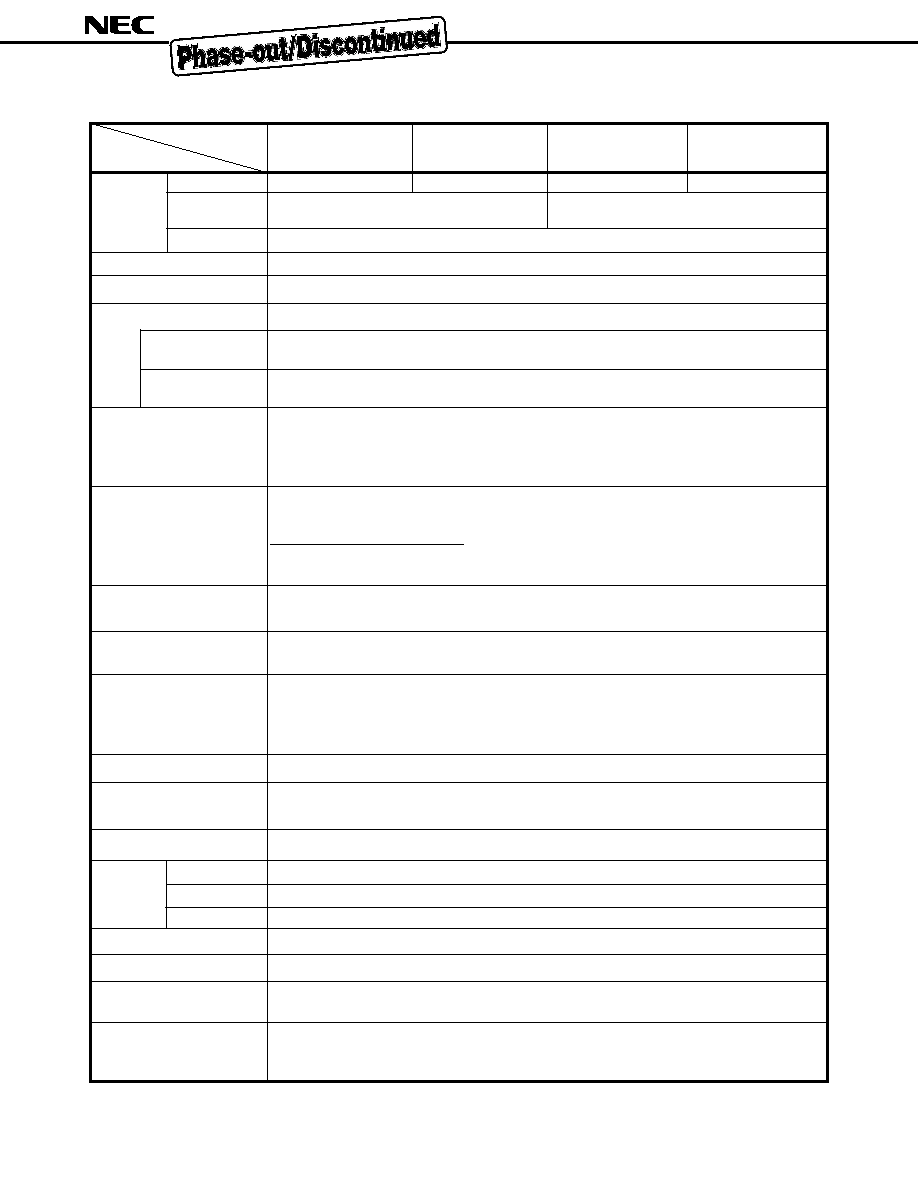
5
PD78011H, 78012H, 78013H, 78014H
8K bytes
16K bytes
24K bytes
32K bytes
32 bytes
64K bytes
8 bits
× 32 registers (8 bits × 8 registers × 4 banks)
On-chip instruction execution time cycle modification function
0.4
s/0.8 s/1.6 s/3.2 s/6.4 s (at 10.0 MHz operation)
122
s (at 32.768 kHz operation)
16-bit operation
Multiplication/division (8 bits
× 8 bits,16 bits ÷ 8 bits)
Bit manipulation (set, reset, test, boolean operation)
BCD correction, etc.
Total
: 53
CMOS input
: 02
CMOS I/O
: 47
N-channel open-drain I/O
(15 V withstand voltage)
: 04
8-bit resolution
× 8 channels
Operable over a wide power supply voltage range: AVDD = 1.8 to 5.5 V
3-wire serial I/O/SBI /2-wire serial I/O mode selectable: 1 channel
3-wire serial I/O mode (on-chip max. 32 bytes automatic data transmit/receive function): 1 channel
16-bit timer/event counter
: 1 channel
8-bit timer/event counter
: 2 channels
Watch timer
: 1 channel
Watchdog timer
: 1 channel
3 (14-bit PWM output
× 1)
39.1 kHz, 78.1 kHz, 156 kHz, 313 kHz, 625 kHz, 1.25 MHz (at main system clock: 10.0 MHz
operation), 32.768 kHz (at subsystem clock: 32.768 kHz operation)
2.4 kHz, 4.9 kHz, 9.8 kHz (at main system clock: 10.0 MHz operation)
Internal
: 8, External : 4
Internal
: 1
1
Internal
: 1, External : 1
VDD = 1.8 to 5.5 V
TA = –40 to +85
°C
64-pin plastic shrink DIP (750 mil)
64-pin plastic QFP (14
× 14 mm)
64-pin plastic LQFP (12
× 12 mm)
Internal
memory
OVERVIEW OF FUNCTION
Product Name
ROM
High-speed
RAM
Buffer RAM
512 bytes
1024 bytes
PD78011H
PD78012H
PD78013H
PD78014H
Item
Memory space
General-purpose registers
Instruction cycle
When main system
clock selected
When subsystem
clock selected
Instruction set
I/O ports
A/D converter
Serial interface
Timer
Timer output
Clock output
Buzzer output
Vectored
interrupt
sources
Test input
Supply voltage
Operating ambient
temperature
Maskable
Non-maskable
Software
Package
相關(guān)PDF資料 |
PDF描述 |
|---|---|
| UPD78053GC-XXX-8BT | 8-BIT, MROM, 5 MHz, MICROCONTROLLER, PQFP80 |
| UPD78322GJ-XXX-5BJ | 16-BIT, MROM, 16 MHz, MICROCONTROLLER, PQFP74 |
| UPD789132GS-XXX | 8-BIT, MROM, MICROCONTROLLER, PDSO30 |
| UPD789122UC-XXX-5A4 | 8-BIT, MROM, MICROCONTROLLER, PDSO30 |
| UPL4-NM-150 | INTERCONNECTION DEVICE |
相關(guān)代理商/技術(shù)參數(shù) |
參數(shù)描述 |
|---|---|
| UPD780134GK-424-9ET-E3-A | 制造商:Renesas Electronics Corporation 功能描述: |
| UPD78014GC-765-AB8 | 制造商:NEC Electronics Corporation 功能描述: |
| UPD78043A041 | 制造商:Panasonic Industrial Company 功能描述:IC |
| UPD78043A042 | 制造商:Panasonic Industrial Company 功能描述:IC |
| UPD78043F016 | 制造商:Panasonic Industrial Company 功能描述:IC |
發(fā)布緊急采購,3分鐘左右您將得到回復(fù)。