- 您現(xiàn)在的位置:買賣IC網(wǎng) > PDF目錄368672 > TMS320UVC5402 (Texas Instruments, Inc.) Fixed-Point Digital Signal Processor(定點(diǎn)DSP) PDF資料下載
參數(shù)資料
| 型號(hào): | TMS320UVC5402 |
| 廠商: | Texas Instruments, Inc. |
| 元件分類: | 數(shù)字信號(hào)處理 |
| 英文描述: | Fixed-Point Digital Signal Processor(定點(diǎn)DSP) |
| 中文描述: | 定點(diǎn)數(shù)字信號(hào)處理器(定點(diǎn)DSP)的 |
| 文件頁(yè)數(shù): | 8/60頁(yè) |
| 文件大?。?/td> | 772K |
| 代理商: | TMS320UVC5402 |
第1頁(yè)第2頁(yè)第3頁(yè)第4頁(yè)第5頁(yè)第6頁(yè)第7頁(yè)當(dāng)前第8頁(yè)第9頁(yè)第10頁(yè)第11頁(yè)第12頁(yè)第13頁(yè)第14頁(yè)第15頁(yè)第16頁(yè)第17頁(yè)第18頁(yè)第19頁(yè)第20頁(yè)第21頁(yè)第22頁(yè)第23頁(yè)第24頁(yè)第25頁(yè)第26頁(yè)第27頁(yè)第28頁(yè)第29頁(yè)第30頁(yè)第31頁(yè)第32頁(yè)第33頁(yè)第34頁(yè)第35頁(yè)第36頁(yè)第37頁(yè)第38頁(yè)第39頁(yè)第40頁(yè)第41頁(yè)第42頁(yè)第43頁(yè)第44頁(yè)第45頁(yè)第46頁(yè)第47頁(yè)第48頁(yè)第49頁(yè)第50頁(yè)第51頁(yè)第52頁(yè)第53頁(yè)第54頁(yè)第55頁(yè)第56頁(yè)第57頁(yè)第58頁(yè)第59頁(yè)第60頁(yè)
TMS320UVC5402
FIXED-POINT DIGITAL SIGNAL PROCESSOR
SPRS100A – APRIL 1999 – REVISED AUGUST 1999
8
POST OFFICE BOX 1443
HOUSTON, TEXAS 77251–1443
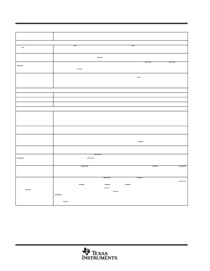
Terminal Functions (Continued)
NAME
DESCRIPTION
TYPE
TERMINAL
HOST-PORT INTERFACE SIGNALS (CONTINUED)
HR/W
I
Read/write. HR/W controls the direction of an HPI transfer. HR/W has an internal pullup resistor that is only
enabled when HPIENA = 0.
HRDY
O/Z
Ready. The ready output informs the host when the HPI is ready for the next transfer. HRDY goes into the
high-impedance state when EMU1/OFF is low.
Interrupt. This output is used to interrupt the host. When the DSP is in reset, HINT is driven high
.
HINT can also
be configured as the timer 1 output (TOUT1) when the HPI is disabled. The signal goes into the high-impedance
state when EMU1/OFF is low.
HINT
O/Z
HPIENA
I
HPI module select. HPIENA must be driven high during reset to enable the HPI. An internal pulldown resistor
is always active and the HPIENA pin is sampled on the rising edge of RS. If HPIENA is left open or is driven low
during reset, the HPI module is disabled. Once the HPI is disabled, the HPIENA pin has no effect until the
’UVC5402 is reset.
SUPPLY PNS
CVDD
DVDD
VSS
S
+VDD. Dedicated power supply for the core CPU
+VDD. Dedicated power supply for the I/O pins
Ground
S
S
TEST PINS
TCK
I
IEEE standard 1149.1 test clock. TCK is normally a free-running clock signal with a 50% duty cycle. The changes
on the test access port (TAP) of input signals TMS and TDI are clocked into the TAP controller, instruction
register, or selected test data register on the rising edge of TCK. Changes at the TAP output signal (TDO) occur
on the falling edge of TCK.
TDI
I
IEEE standard 1149.1 test data input pin with internal pullup device. TDI is clocked into the selected register
(instruction or data) on a rising edge of TCK.
TDO
O/Z
IEEE standard 1149.1 test data output. The contents of the selected register (instruction or data) are shifted out
of TDO on the falling edge of TCK. TDO is in the high-impedance state except when the scanning of data is in
progress. TDO also goes into the high-impedance state when EMU1/OFF is low.
TMS
I
IEEE standard 1149.1 test mode select. Pin with internal pullup device. This serial control input is clocked into
the TAP controller on the rising edge of TCK.
TRST
I
IEEE standard 1149.1 test reset. TRST, when high, gives the IEEE standard 1149.1 scan system control of the
operations of the device. If TRST is not connected or is driven low, the device operates in its functional mode,
and the IEEE standard 1149.1 signals are ignored. Pin with internal pulldown device.
EMU0
I/O/Z
Emulator 0 pin. When TRST is driven low, EMU0 must be high for activation of the OFF condition. When TRST
is driven high, EMU0 is used as an interrupt to or from the emulator system and is defined as input/output by
way of the IEEE standard 1149.1 scan system.
EMU1/OFF
I/O/Z
Emulator 1 pin/disable all outputs. When TRST is driven high, EMU1/OFF is used as an interrupt to or from the
emulator system and is defined as input/output by way of the IEEE standard 1149.1 scan system. When TRST
is driven low, EMU1/OFF is configured as OFF. The EMU1/OFF signal, when active low, puts all output drivers
into the high-impedance state. Note that OFF is used exclusively for testing and emulation purposes (not for
multiprocessing applications). Therefore, for the OFF feature, the following apply:
TRST = low
EMU0 = high
EMU1/OFF = low
I = input, O = output, Z = high impedance, S = supply
P
相關(guān)PDF資料 |
PDF描述 |
|---|---|
| TMS320VC5409PGE-100 | 16-Bit Digital Signal Processor |
| TMS320VC5409GGU-100 | 16-Bit Digital Signal Processor |
| TMS370C736AFNT | 8-BIT MICROCONTROLLER |
| SE370C758BFZT | 8-BIT MICROCONTROLLER |
| SE370C758BJNT | 8-BIT MICROCONTROLLER |
相關(guān)代理商/技術(shù)參數(shù) |
參數(shù)描述 |
|---|---|
| TMS320V34PJ | 制造商:Texas Instruments 功能描述: |
| TMS320V34PJX2 | 制造商:Rochester Electronics LLC 功能描述:- Bulk 制造商:Texas Instruments 功能描述: |
| TMS320V640AGDK4 | 制造商:Texas Instruments 功能描述:TMS320DM640 548PIN FCBGA PG2.0 400 MHZ - Trays |
| TMS320V640AGNZ4 | 制造商:Texas Instruments 功能描述:TMS320DM640 548PIN FCBGA PG2.0 - Trays |
| TMS320V641AGDK5 | 制造商:Texas Instruments 功能描述:TMS320DM641AGDK PG2 548 PIN FCBGA 500MHZ - Trays |
發(fā)布緊急采購(gòu),3分鐘左右您將得到回復(fù)。