- 您現(xiàn)在的位置:買賣IC網(wǎng) > PDF目錄361947 > TMP320LC2401APZS (Texas Instruments, Inc.) DSP CONTROLLERS PDF資料下載
參數(shù)資料
| 型號: | TMP320LC2401APZS |
| 廠商: | Texas Instruments, Inc. |
| 元件分類: | 數(shù)字信號處理 |
| 英文描述: | DSP CONTROLLERS |
| 中文描述: | DSP控制器 |
| 文件頁數(shù): | 58/134頁 |
| 文件大?。?/td> | 1759K |
| 代理商: | TMP320LC2401APZS |
第1頁第2頁第3頁第4頁第5頁第6頁第7頁第8頁第9頁第10頁第11頁第12頁第13頁第14頁第15頁第16頁第17頁第18頁第19頁第20頁第21頁第22頁第23頁第24頁第25頁第26頁第27頁第28頁第29頁第30頁第31頁第32頁第33頁第34頁第35頁第36頁第37頁第38頁第39頁第40頁第41頁第42頁第43頁第44頁第45頁第46頁第47頁第48頁第49頁第50頁第51頁第52頁第53頁第54頁第55頁第56頁第57頁當(dāng)前第58頁第59頁第60頁第61頁第62頁第63頁第64頁第65頁第66頁第67頁第68頁第69頁第70頁第71頁第72頁第73頁第74頁第75頁第76頁第77頁第78頁第79頁第80頁第81頁第82頁第83頁第84頁第85頁第86頁第87頁第88頁第89頁第90頁第91頁第92頁第93頁第94頁第95頁第96頁第97頁第98頁第99頁第100頁第101頁第102頁第103頁第104頁第105頁第106頁第107頁第108頁第109頁第110頁第111頁第112頁第113頁第114頁第115頁第116頁第117頁第118頁第119頁第120頁第121頁第122頁第123頁第124頁第125頁第126頁第127頁第128頁第129頁第130頁第131頁第132頁第133頁第134頁
TMS320LF2407A,TMS320LF2406A,TMS320LF2403A,TMS320LF2402A
TMS320LC2406A,TMS320LC2404A,TMS320LC2403A,TMS320LC2402A
DSP CONTROLLERS
SPRS145K
JULY 2000
REVISED AUGUST 2005
58
POST OFFICE BOX 1443
HOUSTON, TEXAS 77251
1443
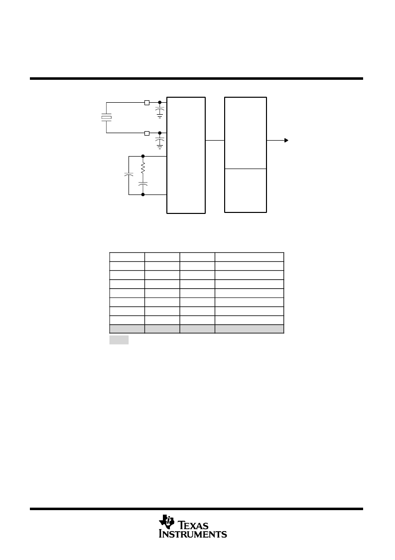
PLL-based clock module (continued)
XTAL2
XTAL1/CLKIN
PLL
XTAL
OSC
CLKOUT
F
in
3-bit
PLL Select
(SCSR1.[11:9])
R
1
C
1
C
2
PLLF
RESONATOR/
CRYSTAL
PLLF2
C
b1
C
b2
Figure 16. PLL Clock Module Block Diagram
Table 9. PLL Clock Selection Through Bits (11
9) in SCSR1 Register
CLK PS2
CLK PS1
CLK PS0
CLKOUT
4
×
F
in
2
×
F
in
1.33
×
F
in
1
×
F
in
0.8
×
F
in
0.66
×
F
in
0.57
×
F
in
0.5
×
F
in
0
0
0
0
0
1
0
1
0
0
1
1
1
0
0
1
0
1
1
1
0
1
1
1
Default multiplication factor after reset is (1,1,1), i.e., 0.5
×
F
in
.
NOTE:
The bootloader sets the PLL to x2 or x4 option. If the bootloader is used, the value of CLKIN used
should not force CLKOUT to exceed the maximum rated device speed. See the “Boot ROM” section
for more details.
external reference crystal clock option
The internal oscillator is enabled by connecting a crystal across the XTAL1/CLKIN and XTAL2 pins as shown
in Figure 17a. The crystal should be in fundamental operation and parallel resonant, with an effective series
resistance of 30
150
and draws no more than 1 mW; it should be specified at a load capacitance of 20 pF.
NOTE: Lx240xA crystal biasing needs an external 1 M
resistor across X1 and X2 pins for reliable operation. See the
TMS320LF2407A,
LF2406A, LF2403A, LF2402A DSP Controllers Silicon Errata
(literature number SPRZ002) or the
TMS320LC2406A, TMS320LC2404A,
TMS320LC2402A DSP Controllers Silicon Errata
(literature number SPRZ185) for details on this requirement.
external reference oscillator clock option
The internal oscillator is disabled by connecting a clock signal to XTAL1/CLKIN and leaving the XTAL2 input
pin unconnected as shown in part b of Figure 17.
相關(guān)PDF資料 |
PDF描述 |
|---|---|
| 5082-7661-CG400 | 7.6 mm (0.3 inch)/10.9 mm (0.43 inch) Seven Segment Displays |
| 74ACT823LMQB | 9-Bit D Flip-Flop |
| 50E-2C-38.0 | TRANS PREBIASED PNP 200MW SOT23 |
| 500E-3CL-5.5 | E Rated Medium Voltage Fuses |
| 500E-3C-5.5 | E Rated Medium Voltage Fuses |
相關(guān)代理商/技術(shù)參數(shù) |
參數(shù)描述 |
|---|---|
| TMP320LC2401AVFA | 制造商:TI 制造商全稱:Texas Instruments 功能描述:DSP CONTROLLERS |
| TMP320LC2401AVFS | 制造商:TI 制造商全稱:Texas Instruments 功能描述:DSP CONTROLLERS |
| TMP320LC2402APAGA | 制造商:未知廠家 制造商全稱:未知廠家 功能描述:DSP|16-BIT|CMOS|TQFP|64PIN|PLASTIC |
| TMP320LC2402APAGS | 制造商:未知廠家 制造商全稱:未知廠家 功能描述:DSP|16-BIT|CMOS|TQFP|64PIN|PLASTIC |
| TMP320LC2402APGA | 制造商:未知廠家 制造商全稱:未知廠家 功能描述:DSP|16-BIT|CMOS|QFP|64PIN|PLASTIC |
發(fā)布緊急采購,3分鐘左右您將得到回復(fù)。