- 您現(xiàn)在的位置:買賣IC網(wǎng) > PDF目錄361947 > TMP320LC2401APZS (Texas Instruments, Inc.) DSP CONTROLLERS PDF資料下載
參數(shù)資料
| 型號: | TMP320LC2401APZS |
| 廠商: | Texas Instruments, Inc. |
| 元件分類: | 數(shù)字信號處理 |
| 英文描述: | DSP CONTROLLERS |
| 中文描述: | DSP控制器 |
| 文件頁數(shù): | 21/134頁 |
| 文件大?。?/td> | 1759K |
| 代理商: | TMP320LC2401APZS |
第1頁第2頁第3頁第4頁第5頁第6頁第7頁第8頁第9頁第10頁第11頁第12頁第13頁第14頁第15頁第16頁第17頁第18頁第19頁第20頁當(dāng)前第21頁第22頁第23頁第24頁第25頁第26頁第27頁第28頁第29頁第30頁第31頁第32頁第33頁第34頁第35頁第36頁第37頁第38頁第39頁第40頁第41頁第42頁第43頁第44頁第45頁第46頁第47頁第48頁第49頁第50頁第51頁第52頁第53頁第54頁第55頁第56頁第57頁第58頁第59頁第60頁第61頁第62頁第63頁第64頁第65頁第66頁第67頁第68頁第69頁第70頁第71頁第72頁第73頁第74頁第75頁第76頁第77頁第78頁第79頁第80頁第81頁第82頁第83頁第84頁第85頁第86頁第87頁第88頁第89頁第90頁第91頁第92頁第93頁第94頁第95頁第96頁第97頁第98頁第99頁第100頁第101頁第102頁第103頁第104頁第105頁第106頁第107頁第108頁第109頁第110頁第111頁第112頁第113頁第114頁第115頁第116頁第117頁第118頁第119頁第120頁第121頁第122頁第123頁第124頁第125頁第126頁第127頁第128頁第129頁第130頁第131頁第132頁第133頁第134頁
TMS320LF2407A,TMS320LF2406A,TMS320LF2403A,TMS320LF2402A
TMS320LC2406A,TMS320LC2404A,TMS320LC2403A,TMS320LC2402A
DSP CONTROLLERS
SPRS145K
JULY 2000
REVISED AUGUST 2005
21
POST OFFICE BOX 1443
HOUSTON, TEXAS 77251
1443
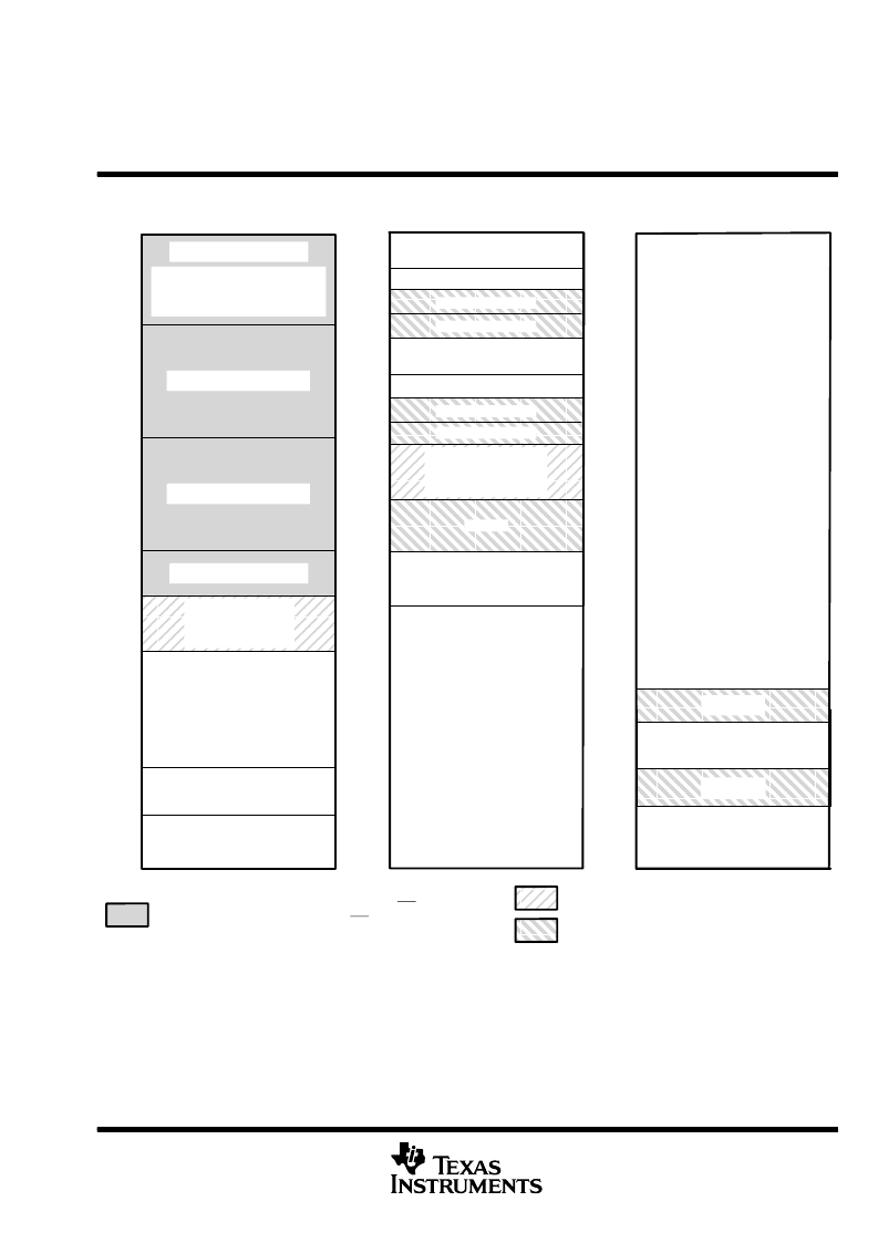
memory maps
èèèèèèèèè
èèèèèèèèè
èèèèèèèèè
Wait-State Generator Control
Register (On-Chip)
èèèèèèèèè
èèèèèèèèè
èèèèèèèèè
èèèèèèèèè
èèèèèèèèè
On-Chip DARAM (B0)§ (CNF = 0)
Reserved (CNF = 1)
ééééééééé
ééééééééé
èèèèèèèèè
èèèèèèèèè
èèèèèèèèè
èèèèèèèèè
Peripheral Memory-Mapped
Registers (System, WD, ADC,
SCI, SPI, CAN, I/O, Interrupts)
ééééééééé
ééééééééé
ééééééééé
Reserved
0000
Hex
Program
On-Chip Flash Memory (Sectored)
if MP/MC = 0
External Program Memory
if MP/MC = 1
7FFF
8000
0000
005F
0060
007F
0080
00FF
0100
Hex
Data
Memory-Mapped
Registers/Reserved Addresses
01FF
0200
02FF
0300
03FF
0400
04FF
0500
èèèèèèèèè
èèèèèèèèè
èèèèèèèèè
SARAM (2K)
Internal (DON = 1)
On-Chip DARAM (B1)
07FF
0800
6FFF
7000
7FFF
8000
External
0000
Hex
I/O
FEFF
FF00
FF0E
FF0F
External
FFFF
FEFF
FF00
FDFF
FE00
External
On-Chip DARAM (B0)
(CNF = 1)
External (CNF = 0)
FFFF
FFFE
FF10
Flash Control Mode Register
SARAM
(See Table 1 for details.)
FFFF
SARAM (2K)
87FF
8800
0FFF
1000
3FFF
4000
Flash Sector 1 (12K)
Flash Sector 2 (12K)
Flash Sector 3 (4K)
6FFF
7000
0FFF
1000
ééééééééé
ééé
ééé
èèè
Reserved or Illegal
Flash Sector 0 (4K)
Interrupt Vectors (0000
003Fh)
Reserved
(0040
0043h)
User code begins at 0044h
Reserved
(CNF = 1)
External (CNF = 0)
NOTE A: Boot ROM: If the boot ROM is enabled, then addresses 0000
00FF in the program space will be occupied by boot ROM.
Addresses 0040h
0043h in on-chip program memory are reserved for code security passwords.
When CNF = 1, addresses FE00h
FEFFh and FF00h
FFFFh are mapped to the same physical block (B0) in program-memory space. For
example, a write to FE00h has the same effect as a write to FF00h. For simplicity, addresses FE00h
FEFFh are referred to as reserved when
CNF = 1.
§
When CNF = 0, addresses 0100h
01FFh and 0200h
02FFh are mapped to the same physical block (B0) in data-memory space. For example,
a write to 0100h has the same effect as a write to 0200h. For simplicity, addresses 0100h
01FFh are referred to as reserved.
Addresses 0300h
03FFh and 0400h
04FFh are mapped to the same physical block (B1) in data-memory space. For example, a write to 0400h
has the same effect as a write to 0300h. For simplicity, addresses 0400h
04FFh are referred to as reserved.
Figure 1. TMS320LF2407A Memory Map
相關(guān)PDF資料 |
PDF描述 |
|---|---|
| 5082-7661-CG400 | 7.6 mm (0.3 inch)/10.9 mm (0.43 inch) Seven Segment Displays |
| 74ACT823LMQB | 9-Bit D Flip-Flop |
| 50E-2C-38.0 | TRANS PREBIASED PNP 200MW SOT23 |
| 500E-3CL-5.5 | E Rated Medium Voltage Fuses |
| 500E-3C-5.5 | E Rated Medium Voltage Fuses |
相關(guān)代理商/技術(shù)參數(shù) |
參數(shù)描述 |
|---|---|
| TMP320LC2401AVFA | 制造商:TI 制造商全稱:Texas Instruments 功能描述:DSP CONTROLLERS |
| TMP320LC2401AVFS | 制造商:TI 制造商全稱:Texas Instruments 功能描述:DSP CONTROLLERS |
| TMP320LC2402APAGA | 制造商:未知廠家 制造商全稱:未知廠家 功能描述:DSP|16-BIT|CMOS|TQFP|64PIN|PLASTIC |
| TMP320LC2402APAGS | 制造商:未知廠家 制造商全稱:未知廠家 功能描述:DSP|16-BIT|CMOS|TQFP|64PIN|PLASTIC |
| TMP320LC2402APGA | 制造商:未知廠家 制造商全稱:未知廠家 功能描述:DSP|16-BIT|CMOS|QFP|64PIN|PLASTIC |
發(fā)布緊急采購,3分鐘左右您將得到回復(fù)。