- 您現(xiàn)在的位置:買賣IC網(wǎng) > PDF目錄373631 > TFRA08C13 Ultraframer DS3/E3/DS2/E2/DS1/E1/DS0 PDF資料下載
參數(shù)資料
| 型號(hào): | TFRA08C13 |
| 元件分類: | 通信及網(wǎng)絡(luò) |
| 英文描述: | Ultraframer DS3/E3/DS2/E2/DS1/E1/DS0 |
| 中文描述: | Ultraframer DS3/E3/DS2/E2/DS1/E1/DS0 |
| 文件頁(yè)數(shù): | 62/188頁(yè) |
| 文件大小: | 3047K |
| 代理商: | TFRA08C13 |
第1頁(yè)第2頁(yè)第3頁(yè)第4頁(yè)第5頁(yè)第6頁(yè)第7頁(yè)第8頁(yè)第9頁(yè)第10頁(yè)第11頁(yè)第12頁(yè)第13頁(yè)第14頁(yè)第15頁(yè)第16頁(yè)第17頁(yè)第18頁(yè)第19頁(yè)第20頁(yè)第21頁(yè)第22頁(yè)第23頁(yè)第24頁(yè)第25頁(yè)第26頁(yè)第27頁(yè)第28頁(yè)第29頁(yè)第30頁(yè)第31頁(yè)第32頁(yè)第33頁(yè)第34頁(yè)第35頁(yè)第36頁(yè)第37頁(yè)第38頁(yè)第39頁(yè)第40頁(yè)第41頁(yè)第42頁(yè)第43頁(yè)第44頁(yè)第45頁(yè)第46頁(yè)第47頁(yè)第48頁(yè)第49頁(yè)第50頁(yè)第51頁(yè)第52頁(yè)第53頁(yè)第54頁(yè)第55頁(yè)第56頁(yè)第57頁(yè)第58頁(yè)第59頁(yè)第60頁(yè)第61頁(yè)當(dāng)前第62頁(yè)第63頁(yè)第64頁(yè)第65頁(yè)第66頁(yè)第67頁(yè)第68頁(yè)第69頁(yè)第70頁(yè)第71頁(yè)第72頁(yè)第73頁(yè)第74頁(yè)第75頁(yè)第76頁(yè)第77頁(yè)第78頁(yè)第79頁(yè)第80頁(yè)第81頁(yè)第82頁(yè)第83頁(yè)第84頁(yè)第85頁(yè)第86頁(yè)第87頁(yè)第88頁(yè)第89頁(yè)第90頁(yè)第91頁(yè)第92頁(yè)第93頁(yè)第94頁(yè)第95頁(yè)第96頁(yè)第97頁(yè)第98頁(yè)第99頁(yè)第100頁(yè)第101頁(yè)第102頁(yè)第103頁(yè)第104頁(yè)第105頁(yè)第106頁(yè)第107頁(yè)第108頁(yè)第109頁(yè)第110頁(yè)第111頁(yè)第112頁(yè)第113頁(yè)第114頁(yè)第115頁(yè)第116頁(yè)第117頁(yè)第118頁(yè)第119頁(yè)第120頁(yè)第121頁(yè)第122頁(yè)第123頁(yè)第124頁(yè)第125頁(yè)第126頁(yè)第127頁(yè)第128頁(yè)第129頁(yè)第130頁(yè)第131頁(yè)第132頁(yè)第133頁(yè)第134頁(yè)第135頁(yè)第136頁(yè)第137頁(yè)第138頁(yè)第139頁(yè)第140頁(yè)第141頁(yè)第142頁(yè)第143頁(yè)第144頁(yè)第145頁(yè)第146頁(yè)第147頁(yè)第148頁(yè)第149頁(yè)第150頁(yè)第151頁(yè)第152頁(yè)第153頁(yè)第154頁(yè)第155頁(yè)第156頁(yè)第157頁(yè)第158頁(yè)第159頁(yè)第160頁(yè)第161頁(yè)第162頁(yè)第163頁(yè)第164頁(yè)第165頁(yè)第166頁(yè)第167頁(yè)第168頁(yè)第169頁(yè)第170頁(yè)第171頁(yè)第172頁(yè)第173頁(yè)第174頁(yè)第175頁(yè)第176頁(yè)第177頁(yè)第178頁(yè)第179頁(yè)第180頁(yè)第181頁(yè)第182頁(yè)第183頁(yè)第184頁(yè)第185頁(yè)第186頁(yè)第187頁(yè)第188頁(yè)
Preliminary Data Sheet
October 2000
TFRA08C13 OCTAL T1/E1 Framer
62
L Lucent Technologies Inc.
Signaling Access
(continued)
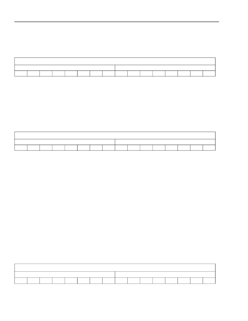
Table 23 illustrates the ASM time-slot format for valid channels.
Table 23. Associated Signaling Mode CHI 2-Byte Time-Slot Format for DS1 Frames
* X indicates bits that are undefined by the framer.
The identical sense of the received system P bit in the transmitted signaling data is echoed back to the system in the received
signaling information.
The DS1 framing formats require rate adaptation from the line-interface 1.544 Mbits/s bit stream to the system-
interface 4.096 Mbits/s bit stream. The rate adaptation results in the need for stuffed time slots on the system inter-
face. Table 24 illustrates the ASM format for T1 stuffed channels used by the TFRA08C13. The stuffed data byte
contains the programmable idle code in register FRM_PR23 (default = 7F (hex)), while the signaling byte is
ignored.
Table 24. Associated Signaling Mode CHI 2-Byte Time-Slot Format for Stuffed Channels
* X indicates bits which are undefined by the framer.
CEPT: Time Slot 16 Signaling
Microprocessor Control Registers
To enable signaling, register FRM_PR44 bit 0 must be set to 0 (default).
The information written into transmit signaling control registers FRM_TSR0—FRM_TSR31 define the state of the
ABCD bits of time slot 16 transmitted to the line.
The received signaling data from time slot 16 is stored in receive signaling registers FRM_RSR0—FRM_RSR31.
Associated Signaling Mode
Signaling information in the associated signaling mode (ASM), register FRM_PR44 bit 2 = 1, is allocated an 8-bit
system time slot in conjunction with the data information for a particular channel. The default system data rate in
the ASM mode is 4.096 Mbits/s. Each system channel consists of an 8-bit payload time slot followed by its associ-
ated 8-bit signaling time slot. The format of the signaling byte is identical to the signaling registers.
Table 25 illustrates the ASM time-slot format for valid CEPT E1 time slots
Table 25. Associated Signaling Mode CHI 2-Byte Time-Slot Format for CEPT
* In the CEPT formats, these bits are undefined.
The P bit is the parity-sense bit calculated over the 8 data bits, the ABCD (and E) bits, and the P bit. The identical sense of the received
system P bit in the transmitted signaling data is echoed back to the system in the received signaling information.
DS1: ASM CHI Time Slot
PAYLOAD DATA
4
SIGNALING INFORMATION*
C
D
1
2
3
5
6
7
8
A
B
X
F
G
P
ASM CHI Time Slot
PAYLOAD DATA
1
SIGNALING INFORMATION*
X
X
0
1
1
1
1
1
1
X
X
X
X
X
X
CEPT ASM CHI Time Slot
PAYLOAD DATA
4
SIGNALING INFORMATION
C
D
1
2
3
5
6
7
8
A
B
E
X
*
X
*
P
相關(guān)PDF資料 |
PDF描述 |
|---|---|
| TFRA08C13 | Ultraframer DS3/E3/DS2/E2/DS1/E1/DS0 |
| TFS380C | VI TELEFILTER Filter specification |
| TFT0675F | Anti-Aliasing and Reconstruction TFT range |
| TFT0675S | Anti-Aliasing and Reconstruction TFT range |
| TFT1350F | Anti-Aliasing and Reconstruction TFT range |
相關(guān)代理商/技術(shù)參數(shù) |
參數(shù)描述 |
|---|---|
| TFRA08C13-DB | 制造商:AGERE 制造商全稱:AGERE 功能描述:TFRA08C13 OCTAL T1/E1 Framer |
| TFRA28J133BAL-1 | 制造商:未知廠家 制造商全稱:未知廠家 功能描述:Telecomm/Datacomm |
| TFRA84J13 | 制造商:AGERE 制造商全稱:AGERE 功能描述:Ultraframer DS3/E3/DS2/E2/DS1/E1/DS0 |
| TFRA84J131BL-3-DB | 制造商:LSI Corporation 功能描述:Framer DS0/DS1/DS2/DS3/E1/E2/E3 1.5V/3.3V 909-Pin BGA |
| TFRA84J13DS0 | 制造商:AGERE 制造商全稱:AGERE 功能描述:Ultraframer DS3/E3/DS2/E2/DS1/E1/DS0 |
發(fā)布緊急采購(gòu),3分鐘左右您將得到回復(fù)。