- 您現(xiàn)在的位置:買賣IC網(wǎng) > PDF目錄368623 > Si9910 (Vishay Intertechnology,Inc.) Adaptive Power MOSFET Driver(可調(diào)功率MOSFET驅(qū)動器) PDF資料下載
參數(shù)資料
| 型號: | Si9910 |
| 廠商: | Vishay Intertechnology,Inc. |
| 英文描述: | Adaptive Power MOSFET Driver(可調(diào)功率MOSFET驅(qū)動器) |
| 中文描述: | 自適應(yīng)功率MOSFET驅(qū)動器(可調(diào)功率MOSFET的驅(qū)動器) |
| 文件頁數(shù): | 3/5頁 |
| 文件大小: | 117K |
| 代理商: | SI9910 |

Si9910
Vishay Siliconix
FaxBack 408-970-5600, request 70009
www.siliconix.com
S-60752—Rev. F, 05-Apr-99
3
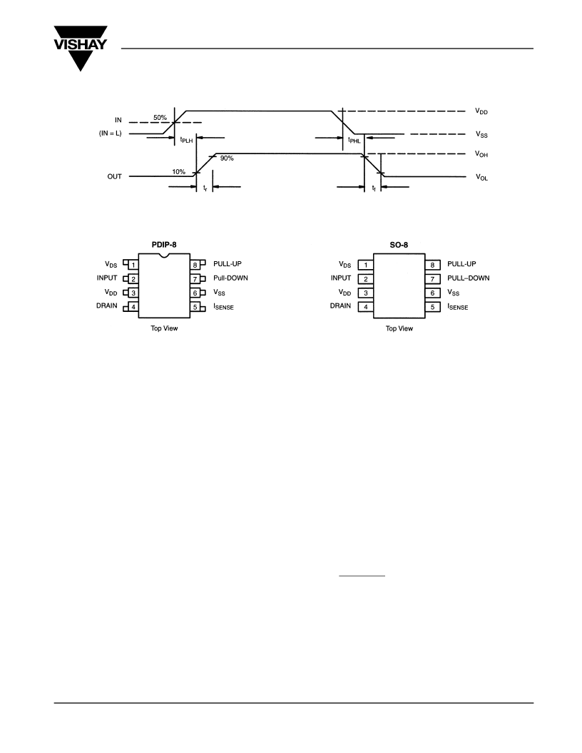
AC TESTING CONDITIONS
PIN CONFIGURATIONS
PIN DESCRIPTION
Pin 1: V
DS
Pin 1 or V
DS
is a sense input for the maximum source-drain
voltage limit. Two microseconds after a high transition on input
pin 2, an internal timer enables the V
DS(max)
sense circuitry. A
catastrophic overcurrent condition, excessive on-resistance,
or insufficient gate-drive voltage can be sensed by limiting
the maximum voltage drop across the power MOSFET. An
external resistor (R3) is required to protect pin 1 from
overvoltage during the MOSFET “off” condition. Exceeding
V
DS(max)
latches the Si9910 “off.” Drive is re-enabled on the
next positive- going input on pin 2. If pin 1 is not used, it must
be connected to pin 6 (V
SS
).
Pin 2: INPUT
A non-inverting, Schmidt trigger input controls the state of the
MOSFET gate-drive outputs and enables the protection logic.
When the input is low (
≤
V
IL
), V
DD
is monitored for an
undervoltage condition (insufficiently charged bootstrap
capacitor). If an undervoltage (
≤
V
DD(min)
) condition exists,
the driver will ignore a turn-on input signal. An undervoltage
(
≤
V
DD(min)
) condition during an “on” state will not be sensed.
Pin 3: V
DD
V
DD
supplies power for the driver’s internal circuitry and
charging current for the power MOSFET’s gate capacitance.
The Si9910 minimizes the internal I
DD
in the
“on” state (gate-
drive outputs high) allowing a “floating” power supply to be
provided by charge pump or bootstrap techniques.
Pin 4: DRAIN
Drain is an analog input to the internal dv/dt limiting circuitry.
An external capacitor (C1) must be used to protect the input
from exposure to the high-voltage (“off” state) drain and to set
the power MOSFET’s maximum rate of dv/dt. If dv/dt feedback
is not used, pin 4 must be left open.
Pin 5: I
SENSE
I
SENSE
in combination with an external resistor (R
1)
protects the power MOSFET from potentially catastrophic
peak currents. I
SENSE
is an analog feedback that limits
current during the power MOSFET’s transition to an “on”
state. It is intended to protect power MOSFETs (in a half-
bridge arrangement) from “shoot-through” current, resulting
from excess di/dt and t
rr
of flyback diodes or from logic timing
overlap. An 0.8-V drop across (R1) should indicate a
current level that is approximately four times the maximum
allowable load current. When the I
SENSE
input is not used, it
should be tied to pin 6 (V
SS
).
Pin 6: V
SS
V
SS
is the driver’s ground return pin. The applications
diagram illustrates the connection of V
SS
for source-
referenced “floating” applications (half-bridge, high-side)
and ground-referenced applications (half-bridge, low-side).
相關(guān)PDF資料 |
PDF描述 |
|---|---|
| SI9926BDY | Dual N-Channel 2.5-V (G-S) MOSFET |
| SI9926ADY | Dual N-Channel 2.5-V (G-S) MOSFET |
| SI9926DY | Dual N-Channel 2.5V Specified PowerTrench MOSFET |
| SI9934BDY | Dual P-Channel 2.5-V (G-S) MOSFET |
| SI9934BDY-T1-E3 | Dual P-Channel 2.5-V (G-S) MOSFET |
相關(guān)代理商/技術(shù)參數(shù) |
參數(shù)描述 |
|---|---|
| SI9910_05 | 制造商:VISHAY 制造商全稱:Vishay Siliconix 功能描述:Adaptive Power MOSFET Driver |
| SI9910DJ | 功能描述:功率驅(qū)動器IC MOSFET Driver RoHS:否 制造商:Micrel 產(chǎn)品:MOSFET Gate Drivers 類型:Low Cost High or Low Side MOSFET Driver 上升時(shí)間: 下降時(shí)間: 電源電壓-最大:30 V 電源電壓-最小:2.75 V 電源電流: 最大功率耗散: 最大工作溫度:+ 85 C 安裝風(fēng)格:SMD/SMT 封裝 / 箱體:SOIC-8 封裝:Tube |
| SI9910DJ-E3 | 功能描述:功率驅(qū)動器IC MOSFET Driver RoHS:否 制造商:Micrel 產(chǎn)品:MOSFET Gate Drivers 類型:Low Cost High or Low Side MOSFET Driver 上升時(shí)間: 下降時(shí)間: 電源電壓-最大:30 V 電源電壓-最小:2.75 V 電源電流: 最大功率耗散: 最大工作溫度:+ 85 C 安裝風(fēng)格:SMD/SMT 封裝 / 箱體:SOIC-8 封裝:Tube |
| SI9910DJ-T1 | 制造商:VISHAY 制造商全稱:Vishay Siliconix 功能描述:Adaptive Power MOSFET Driver1 |
| SI9910DY | 功能描述:功率驅(qū)動器IC MOSFET Driver RoHS:否 制造商:Micrel 產(chǎn)品:MOSFET Gate Drivers 類型:Low Cost High or Low Side MOSFET Driver 上升時(shí)間: 下降時(shí)間: 電源電壓-最大:30 V 電源電壓-最小:2.75 V 電源電流: 最大功率耗散: 最大工作溫度:+ 85 C 安裝風(fēng)格:SMD/SMT 封裝 / 箱體:SOIC-8 封裝:Tube |
發(fā)布緊急采購,3分鐘左右您將得到回復(fù)。