- 您現在的位置:買賣IC網 > PDF目錄98068 > S1C88104P0A0100 8-BIT, MROM, 8.2 MHz, MICROCONTROLLER, PBGA240 PDF資料下載
參數資料
| 型號: | S1C88104P0A0100 |
| 元件分類: | 微控制器/微處理器 |
| 英文描述: | 8-BIT, MROM, 8.2 MHz, MICROCONTROLLER, PBGA240 |
| 封裝: | VFBGA10H-216 |
| 文件頁數: | 124/211頁 |
| 文件大?。?/td> | 1802K |
| 代理商: | S1C88104P0A0100 |
第1頁第2頁第3頁第4頁第5頁第6頁第7頁第8頁第9頁第10頁第11頁第12頁第13頁第14頁第15頁第16頁第17頁第18頁第19頁第20頁第21頁第22頁第23頁第24頁第25頁第26頁第27頁第28頁第29頁第30頁第31頁第32頁第33頁第34頁第35頁第36頁第37頁第38頁第39頁第40頁第41頁第42頁第43頁第44頁第45頁第46頁第47頁第48頁第49頁第50頁第51頁第52頁第53頁第54頁第55頁第56頁第57頁第58頁第59頁第60頁第61頁第62頁第63頁第64頁第65頁第66頁第67頁第68頁第69頁第70頁第71頁第72頁第73頁第74頁第75頁第76頁第77頁第78頁第79頁第80頁第81頁第82頁第83頁第84頁第85頁第86頁第87頁第88頁第89頁第90頁第91頁第92頁第93頁第94頁第95頁第96頁第97頁第98頁第99頁第100頁第101頁第102頁第103頁第104頁第105頁第106頁第107頁第108頁第109頁第110頁第111頁第112頁第113頁第114頁第115頁第116頁第117頁第118頁第119頁第120頁第121頁第122頁第123頁當前第124頁第125頁第126頁第127頁第128頁第129頁第130頁第131頁第132頁第133頁第134頁第135頁第136頁第137頁第138頁第139頁第140頁第141頁第142頁第143頁第144頁第145頁第146頁第147頁第148頁第149頁第150頁第151頁第152頁第153頁第154頁第155頁第156頁第157頁第158頁第159頁第160頁第161頁第162頁第163頁第164頁第165頁第166頁第167頁第168頁第169頁第170頁第171頁第172頁第173頁第174頁第175頁第176頁第177頁第178頁第179頁第180頁第181頁第182頁第183頁第184頁第185頁第186頁第187頁第188頁第189頁第190頁第191頁第192頁第193頁第194頁第195頁第196頁第197頁第198頁第199頁第200頁第201頁第202頁第203頁第204頁第205頁第206頁第207頁第208頁第209頁第210頁第211頁
S1C8F626 TECHNICAL MANUAL
EPSON
13
5 PERIPHERAL CIRCUITS AND THEIR OPERATION (I/O Memory Map)
5 PERIPHERAL CIRCUITS AND
THEIR OPERATION
The peripheral circuits of the S1C8F626 is interfaced with the CPU by means of the memory mapped
I/O method. For this reason, just as with other memory access operations, peripheral circuits can be
controlled by manipulating I/O memory. Below is a description of the operation and control method for
each individual peripheral circuit.
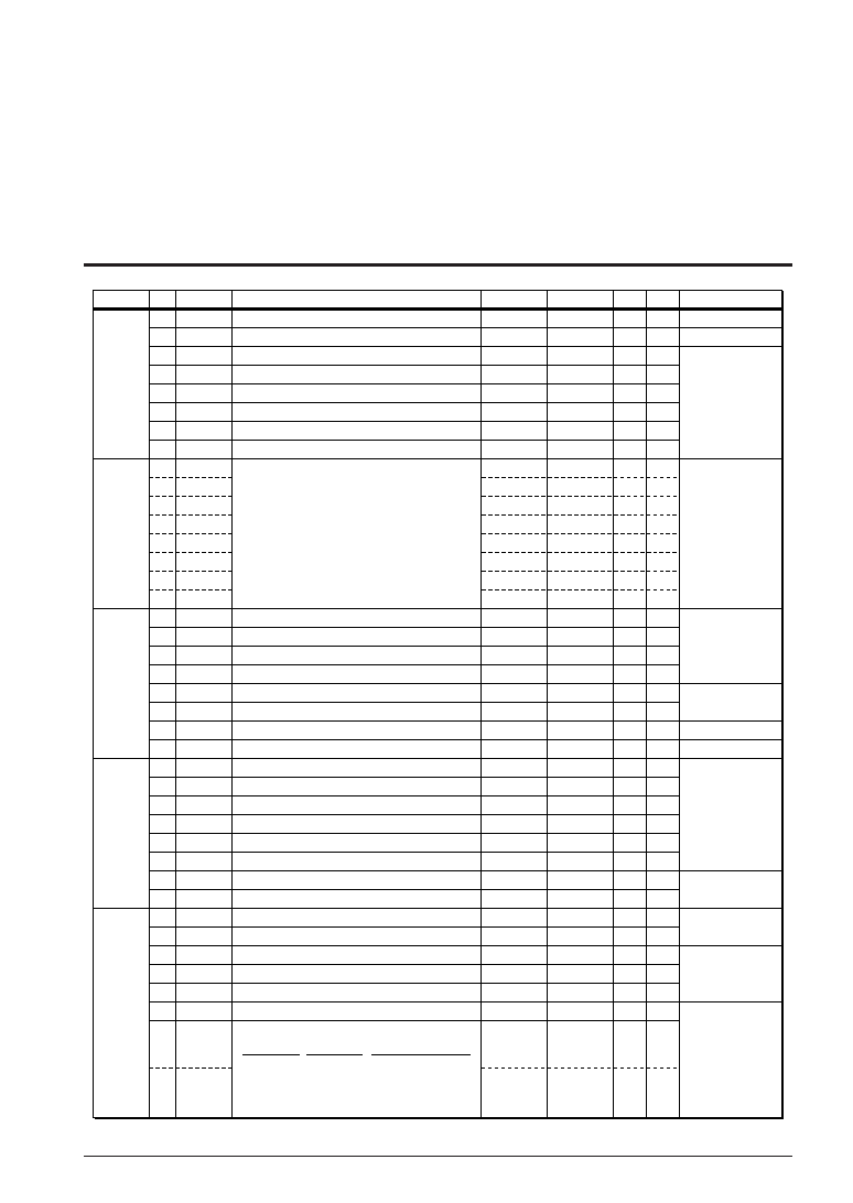
5.1 I/O Memory Map
Table 5.1.1(a) I/O Memory map (00FF00H–00FF10H)
SR R/W
10
Address Bit
Name
Function
Comment
00FF00 D7
D6
D5
D4
D3
D2
D1
D0
–
0
–
R/W
–
CPU mode
–
"0" when being read
Constantly "0" when
being read
–
Maximum
–
Minimum
–
CPUMOD
–
00FF01 D7
D6
D5
D4
D3
D2
D1
D0
SPP7
SPP6
SPP5
SPP4
SPP3
SPP2
SPP1
SPP0
0
R/W
0
Stack pointer page address
1
(MSB)
(LSB)
00FF02 D7
D6
D5
D4
D3
D2
D1
D0
–
CLKCHG
SOSC3
–
VDC
–
1
–
0
R/W
–
OSC3
On
–
VD1 = 2.5 V
–
OSC1
Off
–
VD1 = 1.8 V
–
CPU operating clock switch
OSC3 oscillation On/Off control
–
Operating mode selection
Constantly "0" when
being read
"0" when being read
00FF03 D7
D6
D5
D4
D3
D2
D1
D0
–
0
R/W
–
Power source select for LCD voltage regulator
Power voltage booster On/Off control
Constantly "0" when
being read
–
VD2
On
–
VDD
Off
–
VDSEL
DBON
00FF10 D7
D6
D5
D4
D3
D2
D1
D0
HLMOD
SEGREV
–
DTFNT
LDUTY1
LDUTY0
Heavy load protection mode
Reverse SEG assignment
R/W register
LCD dot font selection
LCD drive duty selection
Reserved register
0
1
0
R/W
On
Reverse
1
12
×12
Off
Normal
0
16
×16/5×8
LDUTY1
1
0
LDUTY0
1
0
1
0
Duty
Not allowed
1/16
1/32
1/8
Note:
____
All the interrupts including NMI are disabled, until you write the optional value into both the 00FF00H and
00FF01H addresses.
相關PDF資料 |
PDF描述 |
|---|---|
| S1C88317D0A0100 | MICROCONTROLLER, UUC170 |
| S1C88308D0A0100 | MICROCONTROLLER, UUC170 |
| S1C88308F0A0100 | MICROCONTROLLER, PQFP160 |
| S1C88348F | 8-BIT, MROM, 8.2 MHz, MICROCONTROLLER, PQFP16 |
| S1C88316D | 8-BIT, MROM, 8.2 MHz, MICROCONTROLLER, UUC172 |
相關代理商/技術參數 |
參數描述 |
|---|---|
| S1C88349 | 制造商:EPSON 制造商全稱:EPSON 功能描述:8-bit Single Chip Microcomputer |
| S1C88649 | 制造商:EPSON 制造商全稱:EPSON 功能描述:8-bit Single Chip Microcomputer |
| S1C88650 | 制造商:EPSON 制造商全稱:EPSON 功能描述:8-bit Single Chip Microcomputer |
| S1C88655 | 制造商:EPSON 制造商全稱:EPSON 功能描述:8-bit Single Chip Microcomputer |
| S1C88816 | 制造商:EPSON 制造商全稱:EPSON 功能描述:8-bit Single Chip Microcomputer |
發(fā)布緊急采購,3分鐘左右您將得到回復。