- 您現(xiàn)在的位置:買賣IC網(wǎng) > PDF目錄368391 > PXASCC (NXP Semiconductors N.V.) CMOS 16-bit communications microcontroller(CMOS 16位通信微控制器) PDF資料下載
參數(shù)資料
| 型號: | PXASCC |
| 廠商: | NXP Semiconductors N.V. |
| 英文描述: | CMOS 16-bit communications microcontroller(CMOS 16位通信微控制器) |
| 中文描述: | 的CMOS 16位微控制器通信的CMOS(16位通信微控制器) |
| 文件頁數(shù): | 7/42頁 |
| 文件大?。?/td> | 229K |
| 代理商: | PXASCC |
第1頁第2頁第3頁第4頁第5頁第6頁當(dāng)前第7頁第8頁第9頁第10頁第11頁第12頁第13頁第14頁第15頁第16頁第17頁第18頁第19頁第20頁第21頁第22頁第23頁第24頁第25頁第26頁第27頁第28頁第29頁第30頁第31頁第32頁第33頁第34頁第35頁第36頁第37頁第38頁第39頁第40頁第41頁第42頁
Philips Semiconductors
Preliminary specification
XA-SCC
CMOS 16-bit communications microcontroller
1999 Mar 29
7
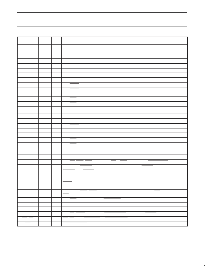
MNEMONIC
NAME AND FUNCTION
TYPE
LQFP
PIN NO.
95
P0.5
1, 2
P0.6
1
P0.7
1
I/O
P0.5_RTClk0_L1Clk
: Port 0 Bit 5, or SCC0 RT clock input, or IDL Clock input.
99
I/O
P0.6_SCPTx
: Port 0 Bit 6, or SCP interface Transmit data output.
100
I/O
P0.7_SCPRx
: Port 0 Bit 7, or SCP interface Receive data input.
TxD0_L1TxD
96
O
TxD0_L1Txd
: Transmit data for SCC0 in NMSI mode, or for IDL bus
RxD0_L1RxD
97
I
RxD0_L1Rxd
: Receive data for SCC0 in NMSI mode, or for IDL bus
SCPClk
98
O
SCPClk
: This output provides the gated clock for the SCP bus.
P1.0
68
I/O
P1.0_RxD2
: Port 1 Bit 0, or SCC2 RxD input
P1.1
P1.2
2
P1.3
2
69
I/O
P1.1_TxD2
: Port 1 Bit 1, or SCC2 TxD output
70
I/O
P1.2_RTClk2
: Port 1 Bit 2, or SCC2 RT Clock input
71
I/O
P1.3_TRClk2
: Port 1 Bit 3, or SCC2 TR Clock input
P1.4
72
I/O
P1.4_CD2
: Port 1 Bit 4, or SCC2 Carrier Detect input
P1.5
73
I/O
P1.5_CTS2
: Port 1 Bit 5, or SCC2 Clear To Send input
P1.6
74
I/O
P1.6_RTS2
: Port 1 Bit 6, or SCC2 Request To Send output
P1.7
75
I/O
P1.7_BRG2_Sync2
: Port 1 Bit 7, or SCC2 Sync input or output, or BRG output, or TxClk output (see
SCC clocks diagrams in User Manual Chp 5)
P2.0
80
I/O
P2.0_RxD3
: Port 2 Bit 0, or SCC3 Rx Data input
P2.1
P2.2
2
P2.3
2
81
I/O
P2.1_TxD3
: Port 2 Bit 1, or SCC3 Tx Data output
82
I/O
P2.2_RTClk3
: Port 2 Bit 2, or SCC3 RT Clock input
83
I/O
P2.3_ComClk_TRClk3
: Port 2 Bit 3, or SCC3 TR Clock input
P2.4
84
I/O
P2.4_CD3
: Port 2 Bit 4, or SCC3 Carrier Detect input
P2.5
85
I/O
P2.5_CTS3
: Port 2 Bit 5, or SCC3 Clear To Send input
P2.6
86
I/O
P2.6_RTS3
: Port 2 Bit 6, or SCC3 Request To Send output
P2.7
87
I/O
P2.7_Sync3_BRG3
: Port 2 Bit 7, or SCC3 Sync input or output, or BRG output, or TxClk output (see
SCC clocks diagrams in User Manual Chp 5)
P3.0
2
56
I/O
P3.0_CS4_RAS4_RTClk1
: Port 3 Bit 0, or CS4 or RAS4 output, or SCC1 RT Clock input
P3.1
57
I/O
P3.1_CS5_RAS5_RTS1
: Port 3 Bit 1, or CS5 or RAS5 output, or SCC1 Request To Send output
P3.2
58
I/O
P3.2_Timer0_ResetOut
: Port 3 Bit 2, or Timer0 input or output, or ResetOut output.
ResetOut
: If the ResetOut function is selected, this pin outputs a low whenever the XA-SCC processor
is reset by an
internal
source (watchdog reset or the RESET instruction.)
WARNING
: Unlike the other
31 GPIO pins, during power up reset, this pin can output a strongly driven low pulse. The duration of this
low pulse ranges from 0ns to 258 system clocks, starting at the time that V
CC
is valid. The state of the
ResetIn pin does not affect this pulse.
When used as GPIO, this pin can also be driven low by software without resetting the XA-SCC.
P3.3
63
I/O
P3.3_Timer1_BRG1_Sync1
: Port 3 Bit 3, or Timer1 input or output, or SCC1 BRG output, or SCC1
Sync input or output
P3.4
64
I/O
P3.4_CTS1
: Port 3 Bit 4, or SCC1 Clear To Send input
P3.5
65
I/O
P3.5_RxD1
: Port 3 Bit 5, or SCC1 Receive Data input
P3.6
P3.7
2
66
I/O
P3.6_TxD1
: Port 3 Bit 6, or SCC1 Transmit Data output
67
I/O
P3.7_Int1_TRClk1
: Port 3 Bit 7, or External Interrupt1 input, or SCC1 TR Clock input
CD1_Int2
Int0
NOTES:
1. See XA-SCC User Guide “Pins Chapter” for how to program selection of pin functions.
2. RTClk input is usually used for Rx Clock if an external clock is needed, but can be used for either Rx or Tx or both. TRClk is usually used for
Tx Clock, but can be used for Rx or Tx or both.
78
I
CD1_Int2
: SCC1 Carrier Detect, or External Interrupt 2
79
I
External Interrupt 0
相關(guān)PDF資料 |
PDF描述 |
|---|---|
| PXASCCKFBE | CMOS 16-bit communications microcontroller |
| PXB9202 | ?Broadband Communication Controller |
| PXC2081 | 480CH 8bit TFT LCD Source Driver with mini-LVDS interface |
| PXC2081COF | 480CH 8bit TFT LCD Source Driver with mini-LVDS interface |
| PXC2081TCP | 480CH 8bit TFT LCD Source Driver with mini-LVDS interface |
相關(guān)代理商/技術(shù)參數(shù) |
參數(shù)描述 |
|---|---|
| PXASCCKFBE | 制造商:PHILIPS 制造商全稱:NXP Semiconductors 功能描述:CMOS 16-bit communications microcontroller |
| PXB 4210 EL V1.2-G | 制造商:Lantiq 功能描述:LTQPXB 4210 EL V1.2-G LQ000001141_GRX288 |
| PXB 4219 E V3.4 | 功能描述:IC ATM/IP INTERWORKING BGA-256 RoHS:否 類別:集成電路 (IC) >> 專用 IC 系列:* 產(chǎn)品培訓(xùn)模塊:Lead (SnPb) Finish for COTS Obsolescence Mitigation Program 標(biāo)準(zhǔn)包裝:1 系列:- 類型:調(diào)幀器 應(yīng)用:數(shù)據(jù)傳輸 安裝類型:表面貼裝 封裝/外殼:400-BBGA 供應(yīng)商設(shè)備封裝:400-PBGA(27x27) 包裝:散裝 |
| PXB 4220 E V3.4-G | 功能描述:IC ATM/IP INTERWORKING BGA-256 RoHS:是 類別:集成電路 (IC) >> 專用 IC 系列:* 產(chǎn)品培訓(xùn)模塊:Lead (SnPb) Finish for COTS Obsolescence Mitigation Program 標(biāo)準(zhǔn)包裝:1 系列:- 類型:調(diào)幀器 應(yīng)用:數(shù)據(jù)傳輸 安裝類型:表面貼裝 封裝/外殼:400-BBGA 供應(yīng)商設(shè)備封裝:400-PBGA(27x27) 包裝:散裝 |
| PXB 4221 E V3.4-G | 功能描述:IC ATM/IP INTERWORKING BGA-256 RoHS:是 類別:集成電路 (IC) >> 專用 IC 系列:* 產(chǎn)品培訓(xùn)模塊:Lead (SnPb) Finish for COTS Obsolescence Mitigation Program 標(biāo)準(zhǔn)包裝:1 系列:- 類型:調(diào)幀器 應(yīng)用:數(shù)據(jù)傳輸 安裝類型:表面貼裝 封裝/外殼:400-BBGA 供應(yīng)商設(shè)備封裝:400-PBGA(27x27) 包裝:散裝 |
發(fā)布緊急采購,3分鐘左右您將得到回復(fù)。