- 您現(xiàn)在的位置:買賣IC網(wǎng) > PDF目錄368391 > PXASCC (NXP Semiconductors N.V.) CMOS 16-bit communications microcontroller(CMOS 16位通信微控制器) PDF資料下載
參數(shù)資料
| 型號: | PXASCC |
| 廠商: | NXP Semiconductors N.V. |
| 英文描述: | CMOS 16-bit communications microcontroller(CMOS 16位通信微控制器) |
| 中文描述: | 的CMOS 16位微控制器通信的CMOS(16位通信微控制器) |
| 文件頁數(shù): | 19/42頁 |
| 文件大?。?/td> | 229K |
| 代理商: | PXASCC |
第1頁第2頁第3頁第4頁第5頁第6頁第7頁第8頁第9頁第10頁第11頁第12頁第13頁第14頁第15頁第16頁第17頁第18頁當(dāng)前第19頁第20頁第21頁第22頁第23頁第24頁第25頁第26頁第27頁第28頁第29頁第30頁第31頁第32頁第33頁第34頁第35頁第36頁第37頁第38頁第39頁第40頁第41頁第42頁
Philips Semiconductors
Preliminary specification
XA-SCC
CMOS 16-bit communications microcontroller
1999 Mar 29
19
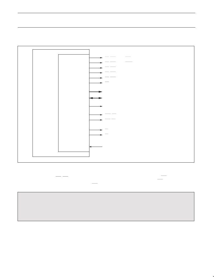
Bus Interface Pins
For this discussion, see Figure 4.
SU01125
CS5, RAS5, (or P3.1, RTS1)
CS4, RAS4, (or P3.0, RTClk1)
CS3, RAS3
CS2, RAS2
CS1, RAS1
CS0
A19–A0 (IF DRAM CYCLE, A22–A0 ARE TIME-MULTIPLEXED FOR RAS/CAS)
D15–D0
ClkOut
CASH, BHE
CASL, BLE
OE
WE
WAIT, SIZE16
XA–SCC
MIF
(MEMORY CONTROLLER)
Figure 4. Memory Bus Interface Signal Pins
Chip Selects and RAS pins
There are six chip select pins (CS5–CS0) mapped to six sets of
bank control registers. The following attributes are individually
programmable for each bank and associated chip select (or RAS if
DRAM): bank on/off, address range, external device access time,
detailed bus strobe sequence, DRAM cycle or generic bus cycle,
DRAM size if DRAM, and bus width. Pin CS0 is always generic in
order to service the boot device, thus CS0 cannot be connected to
DRAM.
WARNING
: On the external bus,
ALL
XA-SCC reads are 16 bit Reads. If the CPU instruction only specifies 8 bits, then the CPU uses
the appropriate byte, and discards the extra byte. Thus “8 Bit Reads” appear to be identical on the bus.
On an 8 bit bus, this will
appear as two consecutive 8 bit reads
even though the CPU instruction specified a byte read
Some 8 bit I/O devices (especially FIFOs) cannot operate correctly with 2 bytes being Read for a 1 Byte Read. The most common (and
least expensive) solution is to operate these 8 bit devices on a 16 bit bus, and access them in software on all odd byte (or all even byte)
boundaries. An added benefit of this technique is that byte reads are faster than on an 8 bit bus, because only 1 word is fetched (a single
read) instead of 2 consecutive bytes.
Clock Output
The CLKOUT pin allows easier external bus interfacing in some
situations. This output reflects the XTALIn clock input to the XA
(referred to internally as CClk or System Clock), but is delayed to
match the external bus outputs and strobes. The default is for
CLKOUT to be output enabled at reset, but it may be turned off
(tri-state disabled) by software via the MICFG MMR.
WARNING:
The capacitive loading on this output must not
exceed 40pf.
相關(guān)PDF資料 |
PDF描述 |
|---|---|
| PXASCCKFBE | CMOS 16-bit communications microcontroller |
| PXB9202 | ?Broadband Communication Controller |
| PXC2081 | 480CH 8bit TFT LCD Source Driver with mini-LVDS interface |
| PXC2081COF | 480CH 8bit TFT LCD Source Driver with mini-LVDS interface |
| PXC2081TCP | 480CH 8bit TFT LCD Source Driver with mini-LVDS interface |
相關(guān)代理商/技術(shù)參數(shù) |
參數(shù)描述 |
|---|---|
| PXASCCKFBE | 制造商:PHILIPS 制造商全稱:NXP Semiconductors 功能描述:CMOS 16-bit communications microcontroller |
| PXB 4210 EL V1.2-G | 制造商:Lantiq 功能描述:LTQPXB 4210 EL V1.2-G LQ000001141_GRX288 |
| PXB 4219 E V3.4 | 功能描述:IC ATM/IP INTERWORKING BGA-256 RoHS:否 類別:集成電路 (IC) >> 專用 IC 系列:* 產(chǎn)品培訓(xùn)模塊:Lead (SnPb) Finish for COTS Obsolescence Mitigation Program 標(biāo)準(zhǔn)包裝:1 系列:- 類型:調(diào)幀器 應(yīng)用:數(shù)據(jù)傳輸 安裝類型:表面貼裝 封裝/外殼:400-BBGA 供應(yīng)商設(shè)備封裝:400-PBGA(27x27) 包裝:散裝 |
| PXB 4220 E V3.4-G | 功能描述:IC ATM/IP INTERWORKING BGA-256 RoHS:是 類別:集成電路 (IC) >> 專用 IC 系列:* 產(chǎn)品培訓(xùn)模塊:Lead (SnPb) Finish for COTS Obsolescence Mitigation Program 標(biāo)準(zhǔn)包裝:1 系列:- 類型:調(diào)幀器 應(yīng)用:數(shù)據(jù)傳輸 安裝類型:表面貼裝 封裝/外殼:400-BBGA 供應(yīng)商設(shè)備封裝:400-PBGA(27x27) 包裝:散裝 |
| PXB 4221 E V3.4-G | 功能描述:IC ATM/IP INTERWORKING BGA-256 RoHS:是 類別:集成電路 (IC) >> 專用 IC 系列:* 產(chǎn)品培訓(xùn)模塊:Lead (SnPb) Finish for COTS Obsolescence Mitigation Program 標(biāo)準(zhǔn)包裝:1 系列:- 類型:調(diào)幀器 應(yīng)用:數(shù)據(jù)傳輸 安裝類型:表面貼裝 封裝/外殼:400-BBGA 供應(yīng)商設(shè)備封裝:400-PBGA(27x27) 包裝:散裝 |
發(fā)布緊急采購,3分鐘左右您將得到回復(fù)。