- 您現(xiàn)在的位置:買賣IC網(wǎng) > PDF目錄367816 > PCF50732 (NXP Semiconductors N.V.) Baseband and audio interface for GSM PDF資料下載
參數(shù)資料
| 型號(hào): | PCF50732 |
| 廠商: | NXP Semiconductors N.V. |
| 英文描述: | Baseband and audio interface for GSM |
| 中文描述: | 用于GSM基帶和音頻接口 |
| 文件頁(yè)數(shù): | 18/64頁(yè) |
| 文件大小: | 322K |
| 代理商: | PCF50732 |
第1頁(yè)第2頁(yè)第3頁(yè)第4頁(yè)第5頁(yè)第6頁(yè)第7頁(yè)第8頁(yè)第9頁(yè)第10頁(yè)第11頁(yè)第12頁(yè)第13頁(yè)第14頁(yè)第15頁(yè)第16頁(yè)第17頁(yè)當(dāng)前第18頁(yè)第19頁(yè)第20頁(yè)第21頁(yè)第22頁(yè)第23頁(yè)第24頁(yè)第25頁(yè)第26頁(yè)第27頁(yè)第28頁(yè)第29頁(yè)第30頁(yè)第31頁(yè)第32頁(yè)第33頁(yè)第34頁(yè)第35頁(yè)第36頁(yè)第37頁(yè)第38頁(yè)第39頁(yè)第40頁(yè)第41頁(yè)第42頁(yè)第43頁(yè)第44頁(yè)第45頁(yè)第46頁(yè)第47頁(yè)第48頁(yè)第49頁(yè)第50頁(yè)第51頁(yè)第52頁(yè)第53頁(yè)第54頁(yè)第55頁(yè)第56頁(yè)第57頁(yè)第58頁(yè)第59頁(yè)第60頁(yè)第61頁(yè)第62頁(yè)第63頁(yè)第64頁(yè)
1999 May 03
18
Philips Semiconductors
Objective specification
Baseband and audio interface for GSM
PCF50732
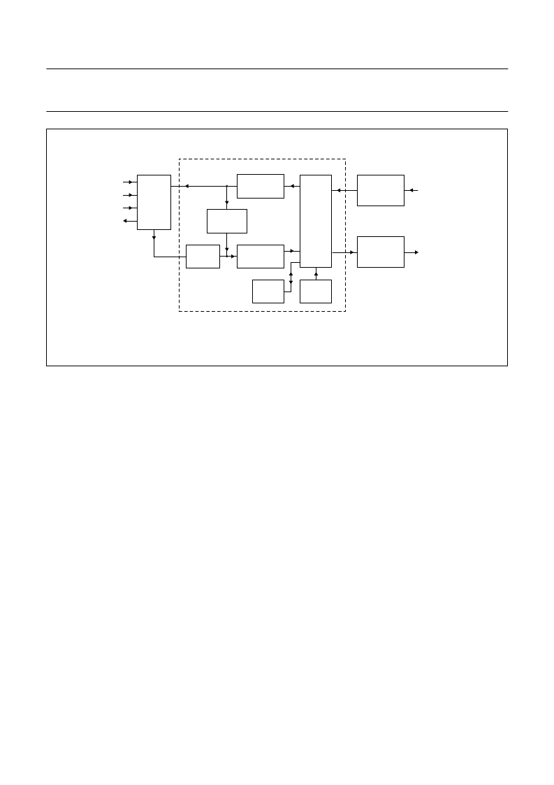
Fig.7 Block diagram of the voice band signal processor.
handbook, full pagewidth
MGR992
DECIMATOR
16-bit, 8 kHz
1-bit, 1 MHz
ASI
ADI
ACLK
AFS
ADO
RX_BS
(receive bitstream)
TX_BS
(transmit bitstream)
RX/TX
FILTER
VOICE BAND SIGNAL PROCESSOR
TXPGA/LIM
RXPGA/LIM
RXVOL
SidePGA
RRAM
IRAM
NOISE
SHAPER
10.3.1
V
OLUME CONTROL BLOCK
The volume control block contains the RXPGA, SidePGA,
TXPGA and both limiter blocks. The possible settings can
be found in the description of the CSI block. All digital
volume control blocks, i.e. RXPGA, SidePGA, and
TXPGA, will allow settings from +6 to
30 dB and mute in
64 steps. However, not all combinations of settings for
these blocks will be meaningful. The limiter will always clip
signals with overflow to the maximum or minimum
allowable value.
10.3.2
A
UDIO
S
ERIAL
I
NTERFACE
(ASI)
BLOCK
The ASI is the voice band serial interface which provides
the connection for the exchange of PCM data in both
receive and transmit directions, between the baseband
digital signal processor and the PCF50732. The data is
coded in 16-bit linear PCM twos complement words.
A frame start is defined by the first falling edge of ACLK
after a rising AFS. This first falling edge is used to clock in
the first data bit on both the baseband and the DSP device.
Data on pin ADI is clocked in (MSB first) on the falling edge
of the ACLK clock. Data is clocked out (MSB first) on pin
ADO on the rising edge of the ACLK clock.
Pin ADO is put in 3-state after the LSB of the transmit
word, independent of the length of the AFS pulse. If the
channel position 0 (see Section 10.3.2.1) is selected, then
the MSB must be output directly after AFS becomes a
logic 1, even if no rising edge on ACLK has been given yet.
The following modes of operation are programmable:
channel position and ACLK clock mode.
10.3.2.1
Channel position mode
Depending on a programmable register value n
(n = 0 to 15) one of 16 channels can be selected (see
Table 22). The ASI can add a delay of 16
×
n-bit clocks
between the assertion of AFS and the start of the MSB of
the PCM values. This delay is independently
programmable for transmit and receive mode.
10.3.2.2
ACLK clock mode
Single or double clock mode can be selected. Double clock
mode implies two clock pulses per data bit and is used for
communication with IOM2 compatible devices. In double
clock mode data must be output on the first rising edge and
be read on the last falling edge.
相關(guān)PDF資料 |
PDF描述 |
|---|---|
| PCF50732H | Baseband and audio interface for GSM |
| PCF7991AT | Advanced Basestation IC, ABIC |
| PCF80C31BH4-24H | CMOS single-chip 8-bit microcontrollers |
| PCB80C51BH-2H | CMOS single-chip 8-bit microcontrollers |
| PCB80C51BH-2P | CMOS single-chip 8-bit microcontrollers |
相關(guān)代理商/技術(shù)參數(shù) |
參數(shù)描述 |
|---|---|
| PCF50732H | 制造商:PHILIPS 制造商全稱:NXP Semiconductors 功能描述:Baseband and audio interface for GSM |
| PCF5075 | 制造商:未知廠家 制造商全稱:未知廠家 功能描述:Power Control/Management |
| PCF5075TDK-T | 制造商:未知廠家 制造商全稱:未知廠家 功能描述:Power Control/Management |
| PCF5077T | 制造商:PHILIPS 制造商全稱:NXP Semiconductors 功能描述:Power amplifier controller for GSM and PCN systems |
| PCF5078 | 制造商:PHILIPS 制造商全稱:NXP Semiconductors 功能描述:Power amplifier controller for GSM and PCN systems |
發(fā)布緊急采購(gòu),3分鐘左右您將得到回復(fù)。