- 您現(xiàn)在的位置:買賣IC網(wǎng) > PDF目錄369939 > P28F001BX-T70 (INTEL CORP) 1-MBIT (128K x 8) BOOT BLOCK FLASH MEMORY PDF資料下載
參數(shù)資料
| 型號: | P28F001BX-T70 |
| 廠商: | INTEL CORP |
| 元件分類: | PROM |
| 英文描述: | 1-MBIT (128K x 8) BOOT BLOCK FLASH MEMORY |
| 中文描述: | 128K X 8 FLASH 12V PROM, 70 ns, PDIP32 |
| 封裝: | 0.620 X 1.640 INCH, PLASTIC, DIP-32 |
| 文件頁數(shù): | 12/33頁 |
| 文件大小: | 436K |
| 代理商: | P28F001BX-T70 |
第1頁第2頁第3頁第4頁第5頁第6頁第7頁第8頁第9頁第10頁第11頁當(dāng)前第12頁第13頁第14頁第15頁第16頁第17頁第18頁第19頁第20頁第21頁第22頁第23頁第24頁第25頁第26頁第27頁第28頁第29頁第30頁第31頁第32頁第33頁

28F001BX-T/28F001BX-B
BOOT BLOCK PROGRAM AND
ERASE
The boot block is intended to contain secure code
which will minimally bring up a system and control
programming and erase of other blocks of the de-
vice, if needed. Therefore, additional ‘‘lockout’’ pro-
tection is provided to guarantee data integrity. Boot
block program and erase operations are enabled
through high voltage V
HH
on either RP
Y
or OE
Y
,
and the normal program and erase command se-
quences are used. Reference the AC Waveforms for
Program/Erase.
If boot block program or erase is attempted while
RP
Y
is at V
IH
, either the Program Status or Erase
Status bit will be set to ‘‘1’’, reflective of the opera-
tion being attempted and indicating boot block lock.
Program/erase attempts while V
IH
k
RP
Y
k
V
HH
produce spurious results and should not be attempt-
ed.
In-System Operation
For on-board programming, the RP
Y
pin is the most
convenient means of altering the boot block. Before
issuing Program or Erase confirms commands, RP
Y
must transition to V
HH
. Hold RP
Y
at this high volt-
age throughout the program or erase interval (until
after Status Register confirm of successful comple-
tion). At this time, it can return to V
IH
or V
IL
.
290406–7
Bus
Command
Comments
Operation
Write
Program
Setup
Data
e
40H
Address
e
Byte to be
Programmed
Write
Program
Data to be programmed
Address
e
Byte to be
Programmed
Read
Status Register Data.
Toggle OE
Y
or CE
Y
to
update Status Register
Check SR.7
1
e
Ready, 0
e
Busy
Standby
Repeat for subsequent bytes.
Full status check can be done after each byte or after a
sequence of bytes.
Write FFH after the last byte programming operation to
reset the device to Read Array Mode.
Bus
Command
Comments
Operation
Standby
Check SR.3
1
e
V
PP
Low Detect
Standby
Check SR.4
1
e
Byte Program Error
SR.3 MUST be cleared, if set during a program attempt,
before further attempts are allowed by the Write State
Machine.
SR.4 is only cleared by the Clear Status Register
Command, in cases where multiple bytes are
programmed before full status is checked.
If error is detected, clear the Status Register before
attempting retry or other error recovery.
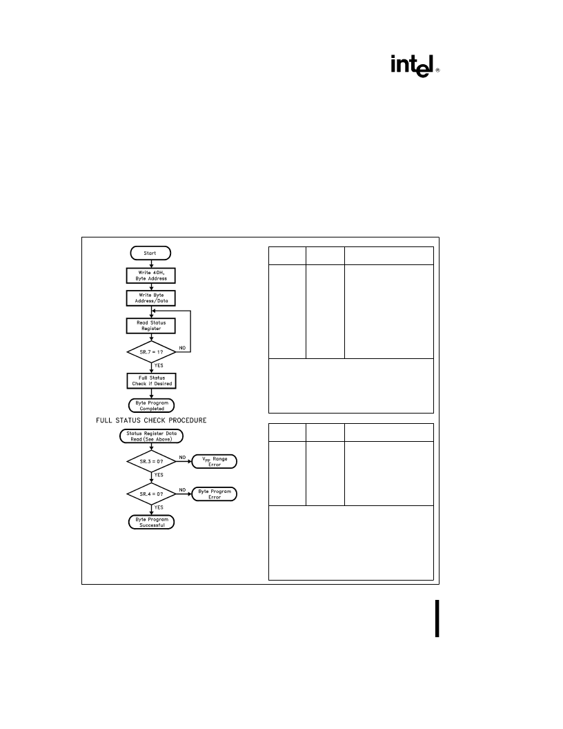
Figure 9. 28F001BX Byte Programming Flowchart
12
相關(guān)PDF資料 |
PDF描述 |
|---|---|
| P28F001BX-T90 | 1-MBIT (128K x 8) BOOT BLOCK FLASH MEMORY |
| P28F001BX-B120 | 1-MBIT (128K x 8) BOOT BLOCK FLASH MEMORY |
| P28F001BX-B150 | 1-MBIT (128K x 8) BOOT BLOCK FLASH MEMORY |
| P28F001BX-B70 | 1-MBIT (128K x 8) BOOT BLOCK FLASH MEMORY |
| P28F001BX-B90 | DB9 MALE TO DB9 FEMALE AME |
相關(guān)代理商/技術(shù)參數(shù) |
參數(shù)描述 |
|---|---|
| P28F001BX-T90 | 制造商:INTEL 制造商全稱:Intel Corporation 功能描述:1-MBIT (128K x 8) BOOT BLOCK FLASH MEMORY |
| P28F002BC-T120 | 制造商:INTEL 制造商全稱:Intel Corporation 功能描述:28F002BC 2-MBIT (256K X 8) BOOT BLOCK FLASH MEMORY |
| P28F002BC-T80 | 制造商:INTEL 制造商全稱:Intel Corporation 功能描述:28F002BC 2-MBIT (256K X 8) BOOT BLOCK FLASH MEMORY |
| P28F010120 | 制造商:Rochester Electronics LLC 功能描述:- Bulk |
| P28F010-120 | 制造商:INTEL 制造商全稱:Intel Corporation 功能描述:28F010 1024K (128K X 8) CMOS FLASH MEMORY |
發(fā)布緊急采購,3分鐘左右您將得到回復(fù)。