- 您現在的位置:買賣IC網 > PDF目錄45388 > MSC8144VT800B (FREESCALE SEMICONDUCTOR INC) 133 MHz, OTHER DSP, PBGA783 PDF資料下載
參數資料
| 型號: | MSC8144VT800B |
| 廠商: | FREESCALE SEMICONDUCTOR INC |
| 元件分類: | 數字信號處理 |
| 英文描述: | 133 MHz, OTHER DSP, PBGA783 |
| 封裝: | 29 X 29 MM, LEAD FREE, PLASTIC, FCPBGA-783 |
| 文件頁數: | 46/80頁 |
| 文件大?。?/td> | 1250K |
| 代理商: | MSC8144VT800B |
第1頁第2頁第3頁第4頁第5頁第6頁第7頁第8頁第9頁第10頁第11頁第12頁第13頁第14頁第15頁第16頁第17頁第18頁第19頁第20頁第21頁第22頁第23頁第24頁第25頁第26頁第27頁第28頁第29頁第30頁第31頁第32頁第33頁第34頁第35頁第36頁第37頁第38頁第39頁第40頁第41頁第42頁第43頁第44頁第45頁當前第46頁第47頁第48頁第49頁第50頁第51頁第52頁第53頁第54頁第55頁第56頁第57頁第58頁第59頁第60頁第61頁第62頁第63頁第64頁第65頁第66頁第67頁第68頁第69頁第70頁第71頁第72頁第73頁第74頁第75頁第76頁第77頁第78頁第79頁第80頁

MSC8144 Quad Core Digital Signal Processor Data Sheet, Rev. 16
Electrical Characteristics
Freescale Semiconductor
50
2.6.5.8
Eye Template Measurements
For the purpose of eye template measurements, the effects of a single-pole high pass filter with a 3 dB point at (baud
frequency)/1667 is applied to the jitter. The data pattern for template measurements is the continuous jitter test pattern (CJPAT)
defined in Annex 48A of IEEE Std. 802.3ae. All lanes of the LP-Serial link shall be active in both the transmit and receive
directions, and opposite ends of the links shall use asynchronous clocks. Four lane implementations shall use CJPAT as defined
in Annex 48A. Single lane implementations shall use the CJPAT sequence specified in Annex 48A for transmission on lane 0.
The amount of data represented in the eye shall be adequate to ensure that the bit error ratio is less than 10–12. The eye pattern
shall be measured with AC coupling and the compliance template centered at 0 Volts differential. The left and right edges of
the template shall be aligned with the mean zero crossing points of the measured data eye. The load for this test shall be 100
Ω
resistive
±5% differential to 2.5 GHz.
2.6.5.9
Jitter Test Measurements
For the purpose of jitter measurement, the effects of a single-pole high pass filter with a 3 dB point at (baud frequency)/1667 is
applied to the jitter. The data pattern for jitter measurements is the Continuous Jitter Test Pattern (CJPAT) pattern defined in
Annex 48A of IEEE Std. 802.3ae. All lanes of the LP-Serial link shall be active in both the transmit and receive directions, and
opposite ends of the links shall use asynchronous clocks. Four lane implementations shall use CJPAT as defined in Annex 48A.
Single lane implementations shall use the CJPAT sequence specified in Annex 48A for transmission on lane 0. Jitter shall be
measured with AC coupling and at 0 V differential. Jitter measurement for the transmitter (or for calibration of a jitter tolerance
setup) shall be performed with a test procedure resulting in a BER curve such as that described in Annex 48B of IEEE Std.
802.3ae.
2.6.5.10
Transmit Jitter
Transmit jitter is measured at the driver output when terminated into a load of 100
Ω resistive ±5% differential to 2.5 GHz.
2.6.5.11
Jitter Tolerance
Jitter tolerance is measured at the receiver using a jitter tolerance test signal. This signal is obtained by first producing the sum
of deterministic and random jitter defined in Section 2.6.5.9 and then adjusting the signal amplitude until the data eye contacts
the 6 points of the minimum eye opening of the receive template shown in Figure 14 and Table 35. Note that for this to occur,
the test signal must have vertical waveform symmetry about the average value and have horizontal symmetry (including jitter)
about the mean zero crossing. Eye template measurement requirements are as defined above. Random jitter is calibrated using
a high pass filter with a low frequency corner at 20 MHz and a 20 dB/decade roll-off below this. The required sinusoidal jitter
specified in Section 8.6 is then added to the signal and the test load is replaced by the receiver being tested.
2.6.6
PCI Timing
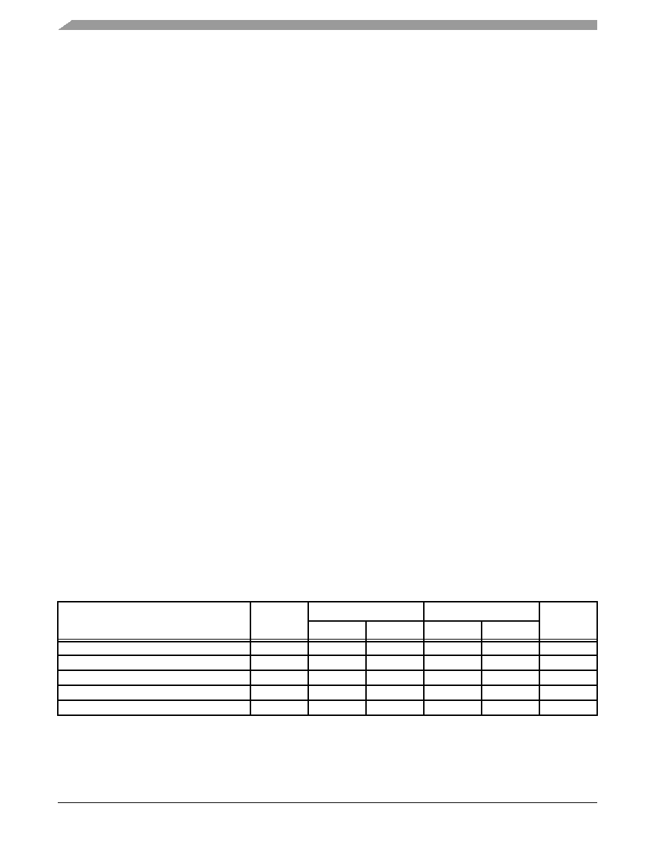
This section describes the general AC timing parameters of the PCI bus. Table 36 provides the PCI AC timing specifications.
Table 36. PCI AC Timing Specifications
Parameter
Symbol
33 MHz
66 MHz
Unit
Min
Max
Min
Max
Output delay
tPCVAL
2.0
11.0
1.0
6.0
ns
High-Z to Valid Output delay
tPCON
2.0
—
1.0
—
ns
Valid to High-Z Output delay
tPCOFF
—
28
—
14
ns
Input setup
tPCSU
7.0
—
3.0
—
ns
Input hold
tPCH
0—0
—
ns
相關PDF資料 |
PDF描述 |
|---|---|
| MSC8144SVT1000A | 133 MHz, OTHER DSP, PBGA783 |
| MSC8144TVT1000A | 133 MHz, OTHER DSP, PBGA783 |
| MSC8144SVT1000B | 133 MHz, OTHER DSP, PBGA783 |
| MSC8144VT1000A | 133 MHz, OTHER DSP, PBGA783 |
| MSC8144SVT800A | 133 MHz, OTHER DSP, PBGA783 |
相關代理商/技術參數 |
參數描述 |
|---|---|
| MSC81450M | 制造商:STMICROELECTRONICS 制造商全稱:STMicroelectronics 功能描述:RF & MICROWAVE TRANSISTORS AVIONICS APPLICATIONS |
| MSC8151 | 制造商:FREESCALE 制造商全稱:Freescale Semiconductor, Inc 功能描述:Single-Core Digital Signal Processor |
| MSC8151SAG1000B | 制造商:Freescale Semiconductor 功能描述:STARCORE DSP, 1X 1GHZ SC3850 CORES, MAPLE-B ACCELERATOR, DDR - Bulk 制造商:Freescale Semiconductor 功能描述:STARCORE DSP, 1X 1GHZ SC3850 CORES, MAPLE-B ACCELERATOR, DDR - Trays 制造商:Freescale Semiconductor 功能描述:IC DSP 1X 1GHZ SC3850 783FCBGA |
| MSC8151SVT1000B | 功能描述:數字信號處理器和控制器 - DSP, DSC Darwin RoHS:否 制造商:Microchip Technology 核心:dsPIC 數據總線寬度:16 bit 程序存儲器大小:16 KB 數據 RAM 大小:2 KB 最大時鐘頻率:40 MHz 可編程輸入/輸出端數量:35 定時器數量:3 設備每秒兆指令數:50 MIPs 工作電源電壓:3.3 V 最大工作溫度:+ 85 C 封裝 / 箱體:TQFP-44 安裝風格:SMD/SMT |
| MSC8151TVT1000B | 功能描述:數字信號處理器和控制器 - DSP, DSC Darwin RoHS:否 制造商:Microchip Technology 核心:dsPIC 數據總線寬度:16 bit 程序存儲器大小:16 KB 數據 RAM 大小:2 KB 最大時鐘頻率:40 MHz 可編程輸入/輸出端數量:35 定時器數量:3 設備每秒兆指令數:50 MIPs 工作電源電壓:3.3 V 最大工作溫度:+ 85 C 封裝 / 箱體:TQFP-44 安裝風格:SMD/SMT |
發(fā)布緊急采購,3分鐘左右您將得到回復。