- 您現(xiàn)在的位置:買賣IC網(wǎng) > PDF目錄25632 > MPC97R73FA (MOTOROLA INC) PLL BASED CLOCK DRIVER, 12 TRUE OUTPUT(S), 0 INVERTED OUTPUT(S), PQFP52 PDF資料下載
參數(shù)資料
| 型號(hào): | MPC97R73FA |
| 廠商: | MOTOROLA INC |
| 元件分類: | 時(shí)鐘及定時(shí) |
| 英文描述: | PLL BASED CLOCK DRIVER, 12 TRUE OUTPUT(S), 0 INVERTED OUTPUT(S), PQFP52 |
| 封裝: | LQFP-52 |
| 文件頁(yè)數(shù): | 14/20頁(yè) |
| 文件大?。?/td> | 252K |
| 代理商: | MPC97R73FA |
第1頁(yè)第2頁(yè)第3頁(yè)第4頁(yè)第5頁(yè)第6頁(yè)第7頁(yè)第8頁(yè)第9頁(yè)第10頁(yè)第11頁(yè)第12頁(yè)第13頁(yè)當(dāng)前第14頁(yè)第15頁(yè)第16頁(yè)第17頁(yè)第18頁(yè)第19頁(yè)第20頁(yè)
MPC97R73
TIMING SOLUTIONS
3
MOTOROLA
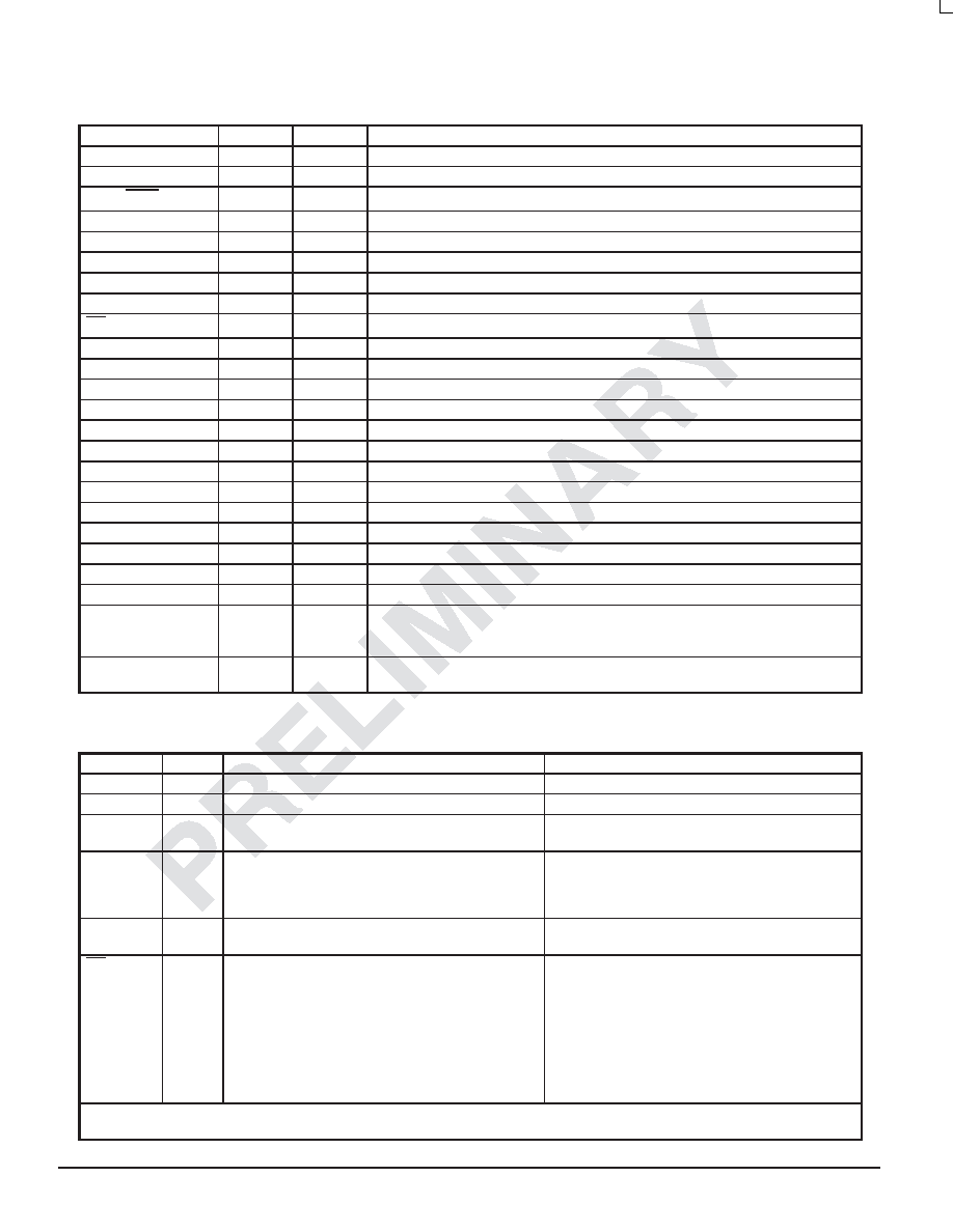
Table 1: PIN CONFIGURATION
Pin
I/O
Type
Function
CCLK0
Input
LVCMOS
PLL reference clock
CCLK1
Input
LVCMOS
Alternative PLL reference clock
PCLK, PCLK
Input
LVPECL
Differential LVPECL reference clock
FB_IN
Input
LVCMOS
PLL feedback signal input, connect to an QFB
CCLK_SEL
Input
LVCMOS
LVCMOS clock reference select
REF_SEL
Input
LVCMOS
LVCMOS/PECL reference clock select
VCO_SEL
Input
LVCMOS
VCO operating frequency select
PLL_EN
Input
LVCMOS
PLL enable/PLL bypass mode select
MR/OE
Input
LVCMOS
Output enable/disable (high-impedance tristate) and device reset
FSEL_A[0:1]
Input
LVCMOS
Frequency divider select for bank A outputs
FSEL_B[0:1]
Input
LVCMOS
Frequency divider select for bank B outputs
FSEL_C[0:1]
Input
LVCMOS
Frequency divider select for bank C outputs
FSEL_FB[0:2]
Input
LVCMOS
Frequency divider select for the QFB output
INV_CLK
Input
LVCMOS
Clock phase selection for outputs QC2 and QC3
STOP_CLK
Input
LVCMOS
Clock input for clock stop circuitry
STOP_DATA
Input
LVCMOS
Configuration data input for clock stop circuitry
QA[0-3]
Output
LVCMOS
Clock outputs (Bank A)
QB[0-3]
Output
LVCMOS
Clock outputs (Bank B)
QC[0-3]
Output
LVCMOS
Clock outputs (Bank C)
QFB
Output
LVCMOS
PLL feedback output. Connect to FB_IN.
QSYNC
Output
LVCMOS
Synchronization pulse output
GND
Supply
Ground
Negative power supply
VCC_PLL
Supply
VCC
PLL positive power supply (analog power supply). It is recommended to use an external
RC filter for the analog power supply pin VCC_PLL. Please see applications section for
details.
VCC
Supply
VCC
Positive power supply for I/O and core. All VCC pins must be connected to the positive
power supply for correct operation
Table 2: FUNCTION TABLE (Configuration Controls)
Control
Default
0
1
REF_SEL
1
Selects CCLKx as the PLL reference clock
Selects the LVPECL inputs as the PLL reference clock
CCLK_SEL
1
Selects CCLK0
Selects CCLK1
VCO_SEL
1
Selects VCO
÷1. (high VCO frequency range)
Selects VCO
÷2. The VCO frequency is scaled by a
factor of 2 (low VCO frequency range).
PLL_EN
1
Test mode with the PLL bypassed. The reference clock
is substituted for the internal VCO output. MPC97R73 is
fully static and no minimum frequency limit applies. All
PLL related AC characteristics are not applicable.
Normal operation mode with PLL enabled.
INV_CLK
1
QC2 and QC3 are in phase with QC0 and QC1
QC2 and QC3 are inverted (180
° phase shift) with
respect to QC0 and QC1
MR/OE
1
Outputs disabled (high-impedance state) and reset of
the device. During reset/output disable the PLL
feedback loop is open and the internal VCO is tied to its
lowest frequency. The MPC97R73 requires reset after
any loss of PLL lock. Loss of PLL lock may occur when
the external feedback path is interrupted. The length of
the reset pulse should be greater than one reference
clock cycle (CCLKx). The device is reset by the internal
power–on reset (POR) circuitry during power–up.
Outputs enabled (active)
VCO_SEL, FSEL_A[0:1], FSEL_B[0:1], FSEL_C[0:1], FSEL_FB[0:2] control the operating PLL frequency range and input/output frequency
ratios. See Table 3 to Table 6 and the applications section for supported frequency ranges and output to input frequency ratios.
相關(guān)PDF資料 |
PDF描述 |
|---|---|
| MPC9892FA | PLL BASED CLOCK DRIVER, 5 TRUE OUTPUT(S), 0 INVERTED OUTPUT(S), PQFP32 |
| MPC9991FA | PLL BASED CLOCK DRIVER, 13 TRUE OUTPUT(S), 0 INVERTED OUTPUT(S), PQFP52 |
| MQ80C154-16P883R | 8-BIT, 16 MHz, MICROCONTROLLER, CQFP44 |
| 952100202 | 8-BIT, 30 MHz, MICROCONTROLLER, CQCC44 |
| MD80C52EXXX-30SBD | 8-BIT, MROM, 30 MHz, MICROCONTROLLER, CDIP40 |
相關(guān)代理商/技術(shù)參數(shù) |
參數(shù)描述 |
|---|---|
| MPC980 | 制造商:MOTOROLA 制造商全稱:Motorola, Inc 功能描述:DUAL 3.3V PLL CLOCK GENERATOR |
| MPC9817 | 制造商:FREESCALE 制造商全稱:Freescale Semiconductor, Inc 功能描述:Clock Generator for PowerQUICC and PowerPC Microprocessors and Microcontrollers |
| MPC9817EN | 功能描述:時(shí)鐘發(fā)生器及支持產(chǎn)品 FSL 1-5 PwrQUICC/Pwr PC Clk Gen, RoHS:否 制造商:Silicon Labs 類型:Clock Generators 最大輸入頻率:14.318 MHz 最大輸出頻率:166 MHz 輸出端數(shù)量:16 占空比 - 最大:55 % 工作電源電壓:3.3 V 工作電源電流:1 mA 最大工作溫度:+ 85 C 安裝風(fēng)格:SMD/SMT 封裝 / 箱體:QFN-56 |
| MPC9817ENR2 | 功能描述:時(shí)鐘發(fā)生器及支持產(chǎn)品 FSL 1-5 PwrQUICC/Pwr PC Clk Gen, RoHS:否 制造商:Silicon Labs 類型:Clock Generators 最大輸入頻率:14.318 MHz 最大輸出頻率:166 MHz 輸出端數(shù)量:16 占空比 - 最大:55 % 工作電源電壓:3.3 V 工作電源電流:1 mA 最大工作溫度:+ 85 C 安裝風(fēng)格:SMD/SMT 封裝 / 箱體:QFN-56 |
| MPC9817SD | 功能描述:時(shí)鐘發(fā)生器及支持產(chǎn)品 FSL 1-5 PwrQUICC/Pwr PC Clk Gen, RoHS:否 制造商:Silicon Labs 類型:Clock Generators 最大輸入頻率:14.318 MHz 最大輸出頻率:166 MHz 輸出端數(shù)量:16 占空比 - 最大:55 % 工作電源電壓:3.3 V 工作電源電流:1 mA 最大工作溫度:+ 85 C 安裝風(fēng)格:SMD/SMT 封裝 / 箱體:QFN-56 |
發(fā)布緊急采購(gòu),3分鐘左右您將得到回復(fù)。