- 您現(xiàn)在的位置:買賣IC網(wǎng) > PDF目錄45359 > MPC8308CVMAFD (FREESCALE SEMICONDUCTOR INC) 32-BIT, 266 MHz, MICROPROCESSOR, PBGA473 PDF資料下載
參數(shù)資料
| 型號(hào): | MPC8308CVMAFD |
| 廠商: | FREESCALE SEMICONDUCTOR INC |
| 元件分類: | 微控制器/微處理器 |
| 英文描述: | 32-BIT, 266 MHz, MICROPROCESSOR, PBGA473 |
| 封裝: | 19 X 19 MM, 0.80 MM PITCH, 1.39 MM HEIGHT, LEAD FREE, MAPBGA-473 |
| 文件頁(yè)數(shù): | 59/88頁(yè) |
| 文件大?。?/td> | 2550K |
| 代理商: | MPC8308CVMAFD |
第1頁(yè)第2頁(yè)第3頁(yè)第4頁(yè)第5頁(yè)第6頁(yè)第7頁(yè)第8頁(yè)第9頁(yè)第10頁(yè)第11頁(yè)第12頁(yè)第13頁(yè)第14頁(yè)第15頁(yè)第16頁(yè)第17頁(yè)第18頁(yè)第19頁(yè)第20頁(yè)第21頁(yè)第22頁(yè)第23頁(yè)第24頁(yè)第25頁(yè)第26頁(yè)第27頁(yè)第28頁(yè)第29頁(yè)第30頁(yè)第31頁(yè)第32頁(yè)第33頁(yè)第34頁(yè)第35頁(yè)第36頁(yè)第37頁(yè)第38頁(yè)第39頁(yè)第40頁(yè)第41頁(yè)第42頁(yè)第43頁(yè)第44頁(yè)第45頁(yè)第46頁(yè)第47頁(yè)第48頁(yè)第49頁(yè)第50頁(yè)第51頁(yè)第52頁(yè)第53頁(yè)第54頁(yè)第55頁(yè)第56頁(yè)第57頁(yè)第58頁(yè)當(dāng)前第59頁(yè)第60頁(yè)第61頁(yè)第62頁(yè)第63頁(yè)第64頁(yè)第65頁(yè)第66頁(yè)第67頁(yè)第68頁(yè)第69頁(yè)第70頁(yè)第71頁(yè)第72頁(yè)第73頁(yè)第74頁(yè)第75頁(yè)第76頁(yè)第77頁(yè)第78頁(yè)第79頁(yè)第80頁(yè)第81頁(yè)第82頁(yè)第83頁(yè)第84頁(yè)第85頁(yè)第86頁(yè)第87頁(yè)第88頁(yè)
MPC8308 PowerQUICC II Pro Processor Hardware Specification, Rev. 1
62
Freescale Semiconductor
Package and Pin Listings
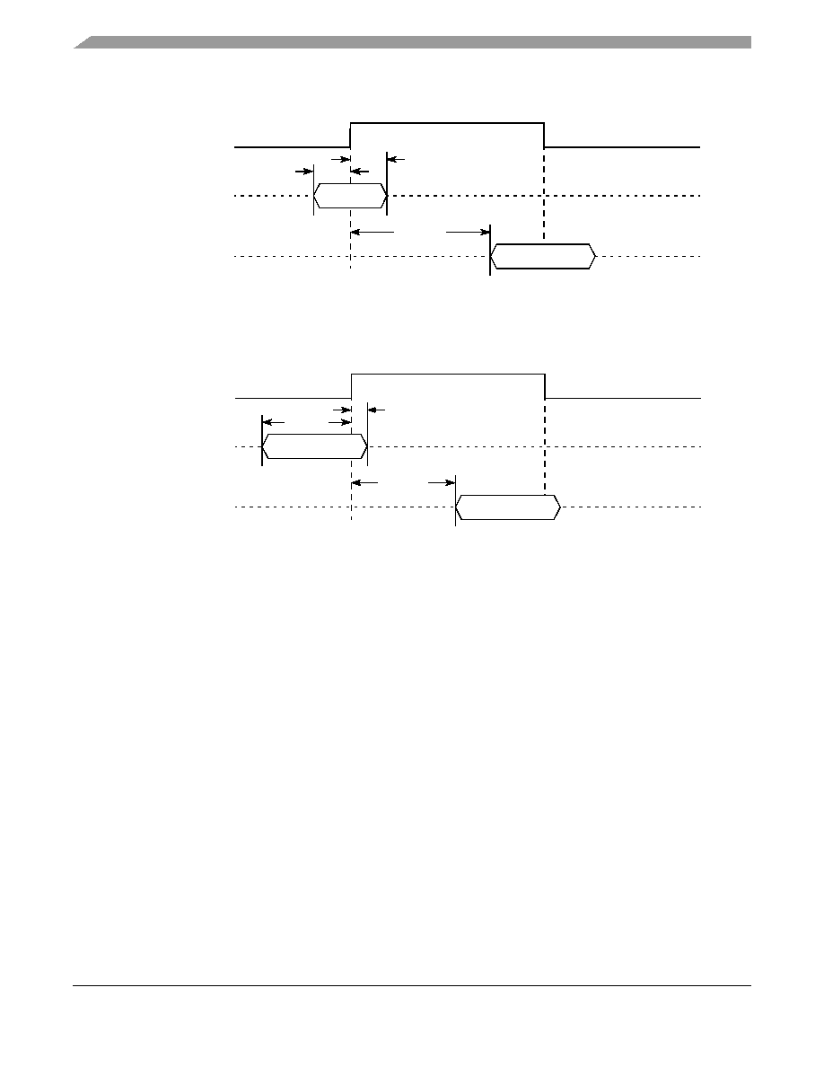
Figure 50 shows the SPI timing in slave mode (external clock).
Figure 50. SPI AC Timing in Slave Mode (External Clock) Diagram
Figure 51 shows the SPI timing in master mode (internal clock).
Figure 51. SPI AC Timing in Master Mode (Internal Clock) Diagram
20 Package and Pin Listings
This section details package parameters, pin assignments, and dimensions. The MPC8308 is available in
a Moulded Array Process Ball Grid Array (MAPBGA). For information on the MAPBGA, see
20.1
Package Parameters for the MPC8308 MAPBGA
The package parameters are as provided in the following list. The package type is 19 mm
× 19 mm, 473
MAPBGA.
Package outline
19 mm
× 19 mm
Interconnects
473
Pitch
0.80 mm
Module height (typical)
1.39 mm
Solder Balls
96.5 Sn/ 3.5Ag
Ball diameter (typical)
0.40 mm
SPICLK (input)
tNEIXKH
tNEIVKH
tNEKHOV
Input Signals:
SPIMOSI
(See Note)
Output Signals:
SPIMISO
(See Note)
Note: The clock edge is selectable on SPI.
SPICLK (output)
tNIIXKH
tNIKHOV
Input Signals:
SPIMISO
(See Note)
Output Signals:
SPIMOSI
(See Note)
Note: The clock edge is selectable on SPI.
tNIIVKH
相關(guān)PDF資料 |
PDF描述 |
|---|---|
| MPC8309CVMAGDCA | 32-BIT, 400 MHz, RISC PROCESSOR, PBGA489 |
| MPC8309CVMADFCA | 32-BIT, 266 MHz, RISC PROCESSOR, PBGA489 |
| MPC8309CVMAHFCA | 32-BIT, 417 MHz, RISC PROCESSOR, PBGA489 |
| MPC8313EVRAFF | 32-BIT, 333 MHz, MICROPROCESSOR, PBGA516 |
| MPC8313EVRAGD | 32-BIT, 400 MHz, MICROPROCESSOR, PBGA516 |
相關(guān)代理商/技術(shù)參數(shù) |
參數(shù)描述 |
|---|---|
| MPC8308CVMAFDA | 功能描述:微處理器 - MPU E300 ext tmp Qual 333 RoHS:否 制造商:Atmel 處理器系列:SAMA5D31 核心:ARM Cortex A5 數(shù)據(jù)總線寬度:32 bit 最大時(shí)鐘頻率:536 MHz 程序存儲(chǔ)器大小:32 KB 數(shù)據(jù) RAM 大小:128 KB 接口類型:CAN, Ethernet, LIN, SPI,TWI, UART, USB 工作電源電壓:1.8 V to 3.3 V 最大工作溫度:+ 85 C 安裝風(fēng)格:SMD/SMT 封裝 / 箱體:FBGA-324 |
| MPC8308CVMAGD | 功能描述:微處理器 - MPU E300 EXT TMP 400 RoHS:否 制造商:Atmel 處理器系列:SAMA5D31 核心:ARM Cortex A5 數(shù)據(jù)總線寬度:32 bit 最大時(shí)鐘頻率:536 MHz 程序存儲(chǔ)器大小:32 KB 數(shù)據(jù) RAM 大小:128 KB 接口類型:CAN, Ethernet, LIN, SPI,TWI, UART, USB 工作電源電壓:1.8 V to 3.3 V 最大工作溫度:+ 85 C 安裝風(fēng)格:SMD/SMT 封裝 / 箱體:FBGA-324 |
| MPC8308CVMAGDA | 功能描述:微處理器 - MPU E300 EXT TMP 400 RoHS:否 制造商:Atmel 處理器系列:SAMA5D31 核心:ARM Cortex A5 數(shù)據(jù)總線寬度:32 bit 最大時(shí)鐘頻率:536 MHz 程序存儲(chǔ)器大小:32 KB 數(shù)據(jù) RAM 大小:128 KB 接口類型:CAN, Ethernet, LIN, SPI,TWI, UART, USB 工作電源電壓:1.8 V to 3.3 V 最大工作溫度:+ 85 C 安裝風(fēng)格:SMD/SMT 封裝 / 箱體:FBGA-324 |
| MPC8308CZQADD | 功能描述:微處理器 - MPU E300 ext tmp Qual266 RoHS:否 制造商:Atmel 處理器系列:SAMA5D31 核心:ARM Cortex A5 數(shù)據(jù)總線寬度:32 bit 最大時(shí)鐘頻率:536 MHz 程序存儲(chǔ)器大小:32 KB 數(shù)據(jù) RAM 大小:128 KB 接口類型:CAN, Ethernet, LIN, SPI,TWI, UART, USB 工作電源電壓:1.8 V to 3.3 V 最大工作溫度:+ 85 C 安裝風(fēng)格:SMD/SMT 封裝 / 箱體:FBGA-324 |
| MPC8308CZQADDA | 功能描述:微處理器 - MPU E300 ext tmp Qual266 RoHS:否 制造商:Atmel 處理器系列:SAMA5D31 核心:ARM Cortex A5 數(shù)據(jù)總線寬度:32 bit 最大時(shí)鐘頻率:536 MHz 程序存儲(chǔ)器大小:32 KB 數(shù)據(jù) RAM 大小:128 KB 接口類型:CAN, Ethernet, LIN, SPI,TWI, UART, USB 工作電源電壓:1.8 V to 3.3 V 最大工作溫度:+ 85 C 安裝風(fēng)格:SMD/SMT 封裝 / 箱體:FBGA-324 |
發(fā)布緊急采購(gòu),3分鐘左右您將得到回復(fù)。