- 您現(xiàn)在的位置:買賣IC網(wǎng) > PDF目錄371014 > MC145202-1 (Motorola, Inc.) PLL Frequency Synthesizer(2.0GHz PLL頻率合成器) PDF資料下載
參數(shù)資料
| 型號: | MC145202-1 |
| 廠商: | Motorola, Inc. |
| 英文描述: | PLL Frequency Synthesizer(2.0GHz PLL頻率合成器) |
| 中文描述: | 鎖相環(huán)頻率合成器(2.0GHz的鎖相環(huán)頻率合成器) |
| 文件頁數(shù): | 17/23頁 |
| 文件大?。?/td> | 270K |
| 代理商: | MC145202-1 |

MC145202–1
DESIGN CONSIDERATIONS
17
MOTOROLA WIRELESS SEMICONDUCTOR
SOLUTIONS – RF AND IF DEVICE DATA
Crystal Oscillator Considerations
The following options may be considered to provide a
reference frequency to Motorola’s CMOS frequency
synthesizers.
Use of a Hybrid Crystal Oscillator
Commercially available temperature–compensated
crystal oscillators (TCXOs) or crystal–controlled data clock
oscillators provide very stable reference frequencies. An
oscillator capable of CMOS logic levels at the output may be
direct or dc coupled to REFin. If the oscillator does not have
CMOS logic levels on the outputs, capacitive or ac coupling
to REFin may be used (see Figure 8).
For additional information about TCXOs and data clock
oscillators, please consult the latest version of the eem
Electronic Engineers Master Catalog,the Gold Book,or
similar publications.
Design an Off–Chip Reference
The user may design an off–chip crystal oscillator using
discrete transistors or ICs specifically developed for crystal
oscillator applications. The reference signal is usually ac
coupled to REFin (see Figure 8). For large amplitude signals
(standard CMOS logic levels), dc coupling may be used.
Use of the On–Chip Oscillator Circuitry
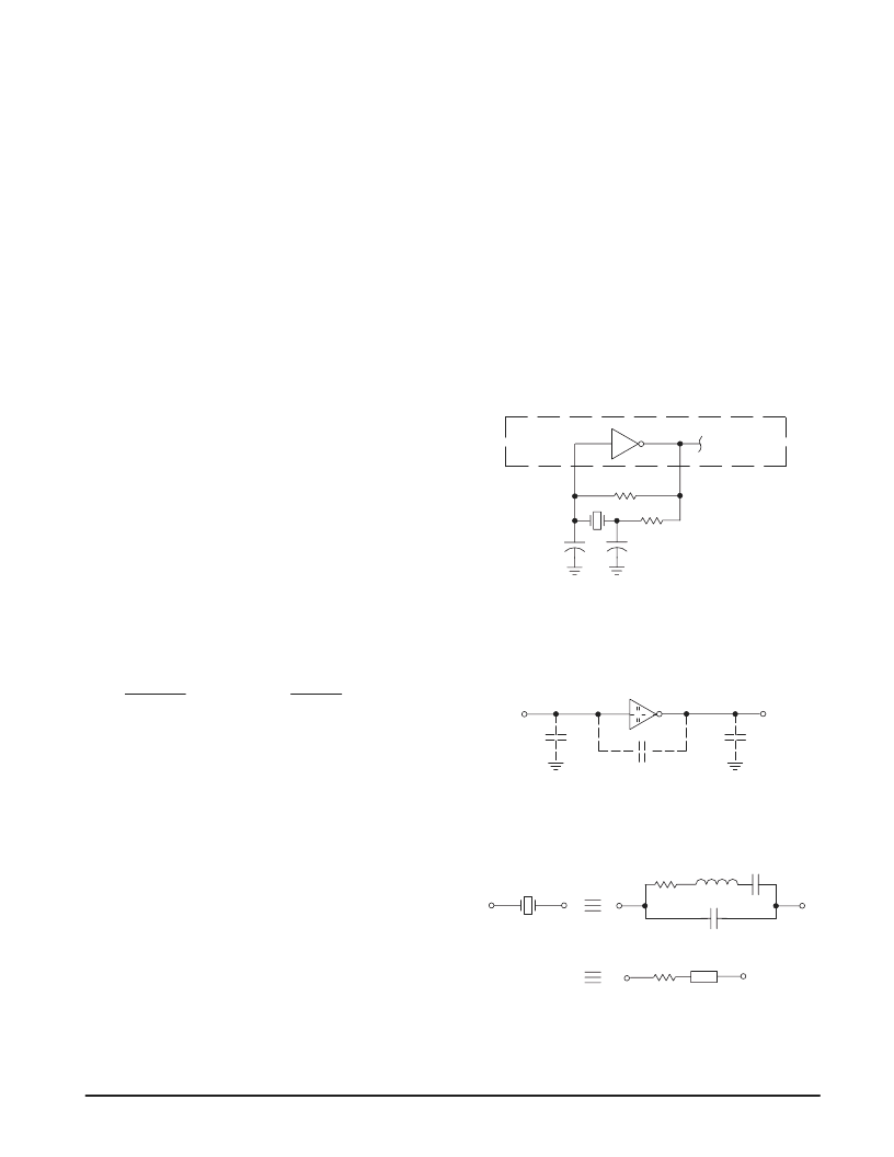
The on–chip amplifier (a digital inverter) along with an
appropriate crystal may be used to provide a reference
source frequency. A fundamental mode crystal, parallel
resonant at the desired operating frequency, should be
connected as shown in Figure 18.
The crystal should be specified for a loading capacitance
(CL) which does not exceed approximately 20 pF when used
at the highest operating frequencies listed in the Loop
Specifications table. Assuming R1 = 0
, the shunt load
capacitance (CL) presented across the crystal can be
estimated to be:
CL =
CinCout
Cin + Cout
+ Ca + Cstray +C1
C2
C1 + C2
where
Cin = 5 pF (see Figure 19)
Cout = 6 pF (see Figure 19)
Ca = 1 pF (see Figure 19)
C1 and C2 = external capacitors (see Figure 18)
Cstray = the total equivalent external circuit stray
capacitance appearing across the crystal
terminals
The oscillator can be “trimmed” on–frequency by making a
portion or all of C1 variable. The crystal and associated
components must be located as close as possible to the
REFin and REFout pins to minimize distortion, stray
capacitance, stray inductance, and startup stabilization time.
Circuit stray capacitance can also be handled by adding the
appropriate stray value to the values for Cin and Cout. For this
approach, the term Cstray becomes 0 in the above expression
for CL.
Power is dissipated in the effective series resistance of the
crystal, Re, in Figure 20. The maximum drive level specified
by the crystal manufacturer represents the maximum stress
that the crystal can withstand without damage or excessive
shift in operating frequency. R1 in Figure 18 limits the drive
level. The use of R1 is not necessary in most cases.
To verify that the maximum dc supply voltage does not
cause the crystal to be overdriven, monitor the output
frequency (fR) at Output A as a function of supply voltage.
(REFout is not used because loading impacts the oscillator.)
The frequency should increase very slightly as the dc supply
voltage is increased. An overdriven crystal decreases in
frequency or becomes unstable with an increase in supply
voltage. The operating supply voltage must be reduced or R1
must be increased in value if the overdriven condition exists.
The user should note that the oscillator start–up time is
proportional to the value of R1.
Through the process of supplying crystals for use with
CMOS inverters, many crystal manufacturers have
developed expertise in CMOS oscillator design with crystals.
Discussions with such manufacturers can prove very helpful
(see Table 7).
R1*
C2
C1
Frequency Synthesizer
REFout
REFin
Rf
* May be needed in certain cases. See text.
Figure 18. Pierce Crystal Oscillator Circuit
Cin
Cout
Ca
REFin
REFout
Cstray
Figure 19. Parasitic Capacitances of the
Amplifier and Cstray
NOTE: Values are supplied by crystal manufacturer
(parallel resonant crystal).
2
1
2
1
2
1
RS
LS
CS
Re
Xe
CO
Figure 20. Equivalent Crystal Networks
相關(guān)PDF資料 |
PDF描述 |
|---|---|
| MC145225 | Dual PLL Frequency Synthesizers With DACs and Voltage Multipliers(帶DACs和電壓乘法器的雙PLL頻率合成器) |
| MC145230 | Dual PLL Frequency Synthesizers With DACs and Voltage Multipliers(帶DACs和電壓乘法器的雙PLL頻率合成器) |
| MC14528BCL | Dual Monostable Multivibrator |
| MC14528 | DEFLECTION PROCESSOR FOR MULTISYNC MONITORS |
| MC14528 | Dual Monostable Multivibrator |
相關(guān)代理商/技術(shù)參數(shù) |
參數(shù)描述 |
|---|---|
| MC14520B | 制造商:Motorola Inc 功能描述: 制造商:ON Semiconductor 功能描述: |
| MC14520BAL | 制造商:Motorola Inc 功能描述:Counter, Up, 4 Bit Binary, 16 Pin, Ceramic, DIP |
| MC14520BCP | 功能描述:計數(shù)器移位寄存器 3-18V Dual BCD Up RoHS:否 制造商:Texas Instruments 計數(shù)器類型: 計數(shù)順序:Serial to Serial/Parallel 電路數(shù)量:1 封裝 / 箱體:SOIC-20 Wide 邏輯系列: 邏輯類型: 輸入線路數(shù)量:1 輸出類型:Open Drain 傳播延遲時間:650 ns 最大工作溫度:+ 125 C 最小工作溫度:- 40 C 封裝:Reel |
| MC14520BCPG | 功能描述:計數(shù)器移位寄存器 3-18V Dual BCD Up RoHS:否 制造商:Texas Instruments 計數(shù)器類型: 計數(shù)順序:Serial to Serial/Parallel 電路數(shù)量:1 封裝 / 箱體:SOIC-20 Wide 邏輯系列: 邏輯類型: 輸入線路數(shù)量:1 輸出類型:Open Drain 傳播延遲時間:650 ns 最大工作溫度:+ 125 C 最小工作溫度:- 40 C 封裝:Reel |
| MC14520BDW | 功能描述:計數(shù)器移位寄存器 3-18V Dual BCD Up RoHS:否 制造商:Texas Instruments 計數(shù)器類型: 計數(shù)順序:Serial to Serial/Parallel 電路數(shù)量:1 封裝 / 箱體:SOIC-20 Wide 邏輯系列: 邏輯類型: 輸入線路數(shù)量:1 輸出類型:Open Drain 傳播延遲時間:650 ns 最大工作溫度:+ 125 C 最小工作溫度:- 40 C 封裝:Reel |
發(fā)布緊急采購,3分鐘左右您將得到回復。