- 您現(xiàn)在的位置:買賣IC網(wǎng) > PDF目錄67763 > M37920F8CHP 16-BIT, FLASH, 20 MHz, MICROCONTROLLER, PQFP100 PDF資料下載
參數(shù)資料
| 型號(hào): | M37920F8CHP |
| 元件分類: | 微控制器/微處理器 |
| 英文描述: | 16-BIT, FLASH, 20 MHz, MICROCONTROLLER, PQFP100 |
| 封裝: | 14 X 14 MM, 0.50 MM PITCH, PLASTIC, LQFP-100 |
| 文件頁(yè)數(shù): | 65/155頁(yè) |
| 文件大?。?/td> | 1274K |
| 代理商: | M37920F8CHP |
第1頁(yè)第2頁(yè)第3頁(yè)第4頁(yè)第5頁(yè)第6頁(yè)第7頁(yè)第8頁(yè)第9頁(yè)第10頁(yè)第11頁(yè)第12頁(yè)第13頁(yè)第14頁(yè)第15頁(yè)第16頁(yè)第17頁(yè)第18頁(yè)第19頁(yè)第20頁(yè)第21頁(yè)第22頁(yè)第23頁(yè)第24頁(yè)第25頁(yè)第26頁(yè)第27頁(yè)第28頁(yè)第29頁(yè)第30頁(yè)第31頁(yè)第32頁(yè)第33頁(yè)第34頁(yè)第35頁(yè)第36頁(yè)第37頁(yè)第38頁(yè)第39頁(yè)第40頁(yè)第41頁(yè)第42頁(yè)第43頁(yè)第44頁(yè)第45頁(yè)第46頁(yè)第47頁(yè)第48頁(yè)第49頁(yè)第50頁(yè)第51頁(yè)第52頁(yè)第53頁(yè)第54頁(yè)第55頁(yè)第56頁(yè)第57頁(yè)第58頁(yè)第59頁(yè)第60頁(yè)第61頁(yè)第62頁(yè)第63頁(yè)第64頁(yè)當(dāng)前第65頁(yè)第66頁(yè)第67頁(yè)第68頁(yè)第69頁(yè)第70頁(yè)第71頁(yè)第72頁(yè)第73頁(yè)第74頁(yè)第75頁(yè)第76頁(yè)第77頁(yè)第78頁(yè)第79頁(yè)第80頁(yè)第81頁(yè)第82頁(yè)第83頁(yè)第84頁(yè)第85頁(yè)第86頁(yè)第87頁(yè)第88頁(yè)第89頁(yè)第90頁(yè)第91頁(yè)第92頁(yè)第93頁(yè)第94頁(yè)第95頁(yè)第96頁(yè)第97頁(yè)第98頁(yè)第99頁(yè)第100頁(yè)第101頁(yè)第102頁(yè)第103頁(yè)第104頁(yè)第105頁(yè)第106頁(yè)第107頁(yè)第108頁(yè)第109頁(yè)第110頁(yè)第111頁(yè)第112頁(yè)第113頁(yè)第114頁(yè)第115頁(yè)第116頁(yè)第117頁(yè)第118頁(yè)第119頁(yè)第120頁(yè)第121頁(yè)第122頁(yè)第123頁(yè)第124頁(yè)第125頁(yè)第126頁(yè)第127頁(yè)第128頁(yè)第129頁(yè)第130頁(yè)第131頁(yè)第132頁(yè)第133頁(yè)第134頁(yè)第135頁(yè)第136頁(yè)第137頁(yè)第138頁(yè)第139頁(yè)第140頁(yè)第141頁(yè)第142頁(yè)第143頁(yè)第144頁(yè)第145頁(yè)第146頁(yè)第147頁(yè)第148頁(yè)第149頁(yè)第150頁(yè)第151頁(yè)第152頁(yè)第153頁(yè)第154頁(yè)第155頁(yè)
M37920F8CGP, M37920F8CHP, M37920FCCGP
M37920FCCHP, M37920FGCGP, M37920FGCHP
17
MITSUBISHI MICROCOMPUTERS
SINGLE-CHIP 16-BIT CMOS MICROCOMPUTER FLASH MEMORY VERSION
PRELIMINAR
Y
Notice:
This
is not
a final
specification.
Some
parametric
limits
are
subject
to change.
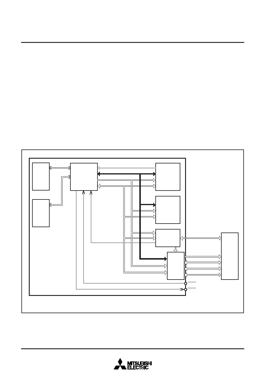
BUS INTERFACE UNIT
Data transfer shown below is always performed via the bus interface
unit (BIU), which is located between the CPU and the internal buses:
Between the CPU and the internal memory, internal peripheral de-
vices, external areas
Between the DMA controller (DMAC) and the internal memory, in-
ternal peripheral devices, external areas
Figure 7 shows the BIU and the bus structure. The CPU and BIU, or
DMAC and BIU are connected by a dedicated bus respectivery, and
any transfer between the CPU and BIU, or DMAC and BIU is con-
trolled by this dedicated bus.
On the other hand, data transfer between the BIU and internal pe-
ripheral devices uses the following internal common buses: 32-bit
code bus, 16-bit data bus, 24-bit address bus, and control signals.
The bus control method where the code bus and the data bus sepa-
rate out (hereafter, this method is referred to as the separate code/
data bus method) is employed in order to improve data transfer ca-
Fig. 7 BIU and bus structure
Internal code bus (CB0 to CB31)
Central
Processing
Unit
(CPU)
SFR : Special Function Register
g The CPU bus, DMAC bus, internal bus, and external bus separate out independently.
External
devices
Internal control signal
CPU bus
Internal bus
Internal data bus (DB0 to DB15)
Internal
memory
Internal
peripheral
devices
(SFR)
External bus
A0 to A23 (MA0 to MA11)
D0 to D7
D8 to D15
Control signal
Bus
Interface
Unit
(BIU)
Bus
conversion
circuit
Internal address bus (AD0 to AD23)
DMA
controller
(DMAC)
DMAC bus
Refresh request
DRAM control signal
DRAM
controller
(DRAMC)
HOLD
Hold request
HLDA
pabilities. As a result, the internal memory is connected to both the
code bus and the data bus, and registers of all other internal periph-
eral devices are connected only to the data bus.
Each width of external buses are as follows: a 24-bit address bus,
16-bit data bus.
The external data bus transfers instruction codes and data. When
the code or data access occurs for the external, the external access
is performed via the bus conversion circuit.
When the DRAM is selected in external devices, the internal DMAC
controller (DRAMC) is operated, and access for DRAM and DRAM
refresh operation become enabled. For details, refer to the section
on the chip select wait controller and DRAMC described later.
When accessing the external devices, it is possible to insert the re-
covery cycles. Refer to the section on the processor modes and chip
select wait controller described later.
When the burst ROM is used as an external device, refer to the sec-
tion on the chip select wait controller described later.
相關(guān)PDF資料 |
PDF描述 |
|---|---|
| M37920F8CGP | 16-BIT, FLASH, 20 MHz, MICROCONTROLLER, PQFP100 |
| M38039MFL-XXXHP | 8-BIT, MROM, 16.8 MHz, MICROCONTROLLER, PQFP64 |
| M38039MFL-XXXSP | 8-BIT, MROM, 16.8 MHz, MICROCONTROLLER, PDIP64 |
| M38039MFL-XXXWG | 8-BIT, MROM, 16.8 MHz, MICROCONTROLLER, PBGA64 |
| M38039FFLHP | 8-BIT, FLASH, 16.8 MHz, MICROCONTROLLER, PQFP64 |
相關(guān)代理商/技術(shù)參數(shù) |
參數(shù)描述 |
|---|---|
| M37920FCCGP | 制造商:MITSUBISHI 制造商全稱:Mitsubishi Electric Semiconductor 功能描述:SINGLE-CHIP 16-BIT CMOS MICROCOMPUTER FLASH MEMORY VERSION |
| M37920FCCHP | 制造商:MITSUBISHI 制造商全稱:Mitsubishi Electric Semiconductor 功能描述:SINGLE-CHIP 16-BIT CMOS MICROCOMPUTER FLASH MEMORY VERSION |
| M37920FGCGP | 制造商:MITSUBISHI 制造商全稱:Mitsubishi Electric Semiconductor 功能描述:SINGLE-CHIP 16-BIT CMOS MICROCOMPUTER FLASH MEMORY VERSION |
| M37920FGCHP | 制造商:MITSUBISHI 制造商全稱:Mitsubishi Electric Semiconductor 功能描述:SINGLE-CHIP 16-BIT CMOS MICROCOMPUTER FLASH MEMORY VERSION |
| M37920S4CGP | 制造商:MITSUBISHI 制造商全稱:Mitsubishi Electric Semiconductor 功能描述:16 BIT CMOS MICROCOMPUTER |
發(fā)布緊急采購(gòu),3分鐘左右您將得到回復(fù)。